Continue to Site

Welcome to EDAboard.com

Welcome to our site! EDAboard.com is an international Electronics Discussion Forum focused on EDA software, circuits, schematics, books, theory, papers, asic, pld, 8051, DSP, Network, RF, Analog Design, PCB, Service Manuals... and a whole lot more! To participate you need to register. Registration is free. Click here to register now.

bias tee circuit problem for balanced amplifier at 2 to 5GHz. Please help me check

Status
Not open for further replies.

Topsy

Newbie level 5
Joined
Jun 20, 2013
Messages
10
Helped
0
Reputation
0
Reaction score
0
Trophy points
1
Activity points
72
bias tee circuit problem for balanced amplifier at 1 to 5GHz. Please help me check

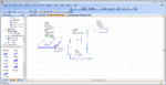
Please i am trying to design a bias Tee circuit for my balanced amplifier design operating at

the frequency range of 1 to 5GHz with centre frequency at 2.4GHz. what value of impedance do you think i can use for the design.

Also where will i attached the DC source to the circuit. Please help. The circuit for the bias is attached.
 

Attachments

  • bias tee.png
    bias tee.png
    67.6 KB · Views: 110
Last edited:

The value for the capacitor should be much less than your Characteristic impedance whereas for inductor it should be higher than characteristic like for example for a Zo=50 Ohm , impedance that capacitor should give be like 2 ohm or so, and inductor will be 500 ohm let say...

Follow this link it will be helpful..
Also Google you can find a lot about bias tee..
 
  • Like
Reactions: @YY

    @YY

    Points: 2
    Helpful Answer Positive Rating
The value for the capacitor should be much less than your Characteristic impedance whereas for inductor it should be higher than characteristic like for example for a Zo=50 Ohm , impedance that capacitor should give be like 2 ohm or so, and inductor will be 500 ohm let say...

Follow this link it will be helpful..
Also Google you can find a lot about bias tee..


Thanks so much, i am going to try it nah

- - - Updated - - -

Owis. that means the inductor reactance is 10times the impedance(500 ohms or more), and the capacitor reactance should be 10% of the impedance (5 Ohms or lower)
 

The value for the capacitor should be much less than your Characteristic impedance whereas for inductor it should be higher than characteristic like for example for a Zo=50 Ohm , impedance that capacitor should give be like 2 ohm or so, and inductor will be 500 ohm let say...

Follow this link it will be helpful..
Also Google you can find a lot about bias tee..

Hi Owe@i$, I have the same problem where i dont understand. I read the link about the bias tee as well. Becuase all this while I thought the cap is functioned as a RF block and the inductor function to control the current flow. would like to know, if i have a wrong inductor so I will have a wrong bias level then? Sorry if my thinking is stupid/naive.
 

@ Topsy

it is not a established rule or formula that value should be this and this much of the impedance.. it is something that i have heard from one of my teacher and i saw few people using it as a thumb rule or estimate u can say ....!!!

@YY

Inductor is there to block the main RF signal from entering in to the source ..... changing the value will change the impedance that it will offer the signal of a particular frequency. Google RF choke and you will find lot of literature on it.
have a look at here also
 
  • Like
Reactions: @YY

    @YY

    Points: 2
    Helpful Answer Positive Rating
@Owis,I just discovered that my inductor is behaving like an idea inductor which is not the same in the real world. Could you please tell me how to deal with the self resonance frequency of the inductor. my frequency ranges from 1 to 5GHz with design frequency of 2.4GHz
 

i decided to check the datasheet of my inductors and chose the inductor value with a resonance frequency above my operating frequency and i use that value to solve for capacitor. now i have a lower value of 33nH and cap of 0.56Pf. what i am not sure of is if my inductor can still act as an rf block and my capacitor blocking the dc
 

How do you concluded that it is behaving ideally ?? :-?

Anyhow bro do some calculation but before, some main points:

1- RF choke (inductor) should provide higher resistance to your whole frequency band but lower resistance comparatively to frequencies outside the band.
2- DC block (Capacitor) conversely should provide higher resistance to DC.

now with the inductor value of 33nH and frequency 2.4GHz use Xl=wL find impedance it will be (497 ohm ~500 ohm) do this again but now with frequency let say 0.1Ghz... your impedance now should be less than previously calculated it is (20 ohm) .. so RF choke is working fine...

Secondly the capacitor is actually a BYpass capacitor means to pass AC from source to ground and leave DC to proceed for Biasing usually for bypass we use 0.1uf 1uf or 100uf Range capacitors.

Thirdly third is the coupling capacitor b/w output of one stage to the input of other.... it should ideally allow the main RF signal to next stage but block any DC level that may cause the shift in next level. its value is also calculated same way with formula Xc=1/wC conversely it should now provide higher impedance to low frequency but low impedance to higher frequency.

Now with these points calculate and design your values then select close standard values that you can find and it will work hopefully ..
 
  • Like
Reactions: Topsy

    Topsy

    Points: 2
    Helpful Answer Positive Rating
Status
Not open for further replies.

Part and Inventory Search

Welcome to EDABoard.com

Sponsor

Back
Top