Continue to Site

Welcome to EDAboard.com

Welcome to our site! EDAboard.com is an international Electronics Discussion Forum focused on EDA software, circuits, schematics, books, theory, papers, asic, pld, 8051, DSP, Network, RF, Analog Design, PCB, Service Manuals... and a whole lot more! To participate you need to register. Registration is free. Click here to register now.

Doubts regarding on Example(C:\ADS2009\examples\MW_Ckt) amplifier Layout in ADS2009.

Status
Not open for further replies.

raju_kambar

Full Member level 3
Joined
Jun 19, 2013
Messages
153
Helped
5
Reputation
10
Reaction score
5
Trophy points
18
Location
Earth
Activity points
1,404
Doubts regarding on Example amplifier Layout in ADS2009.

Dear Sir,
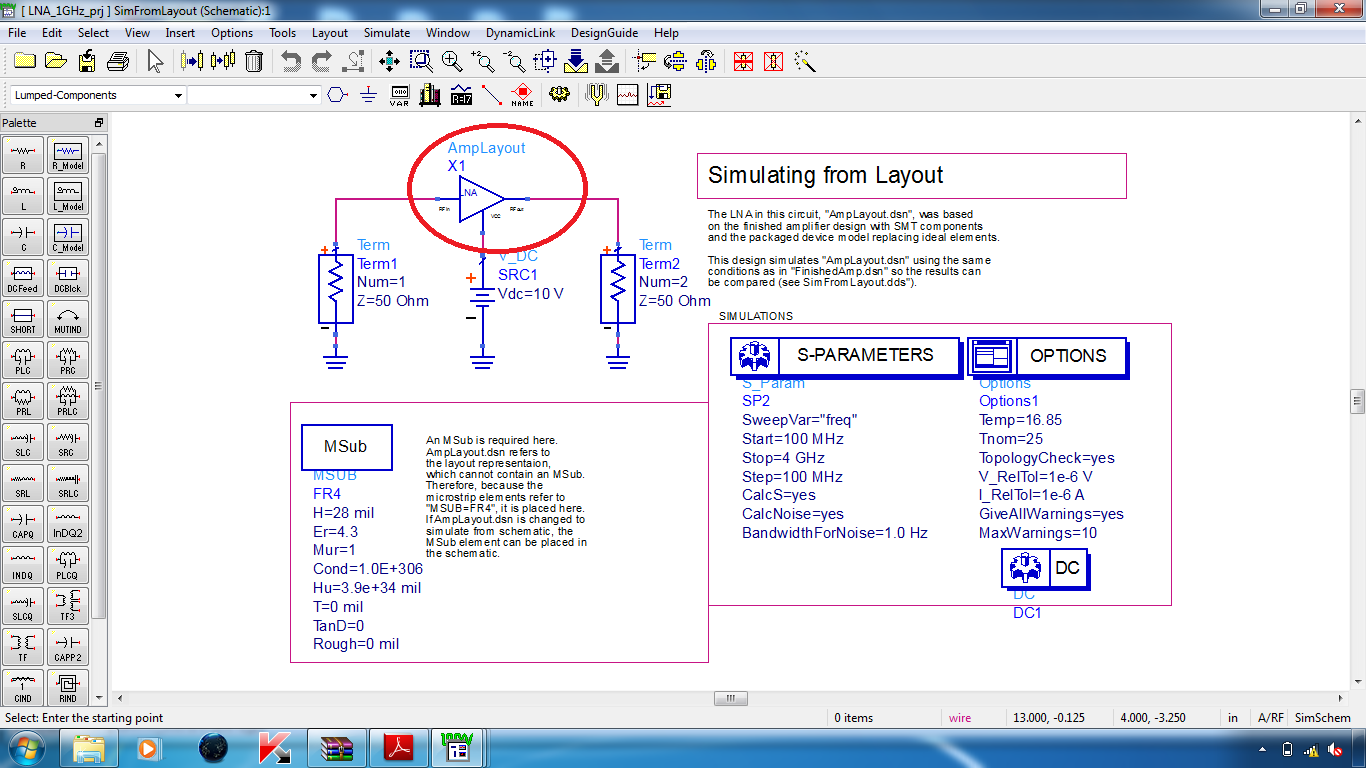
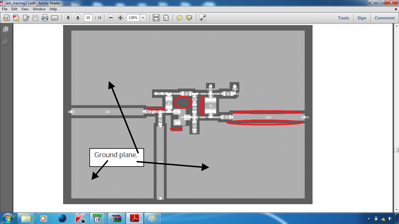
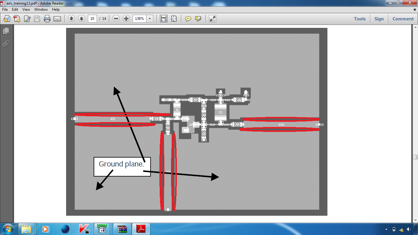
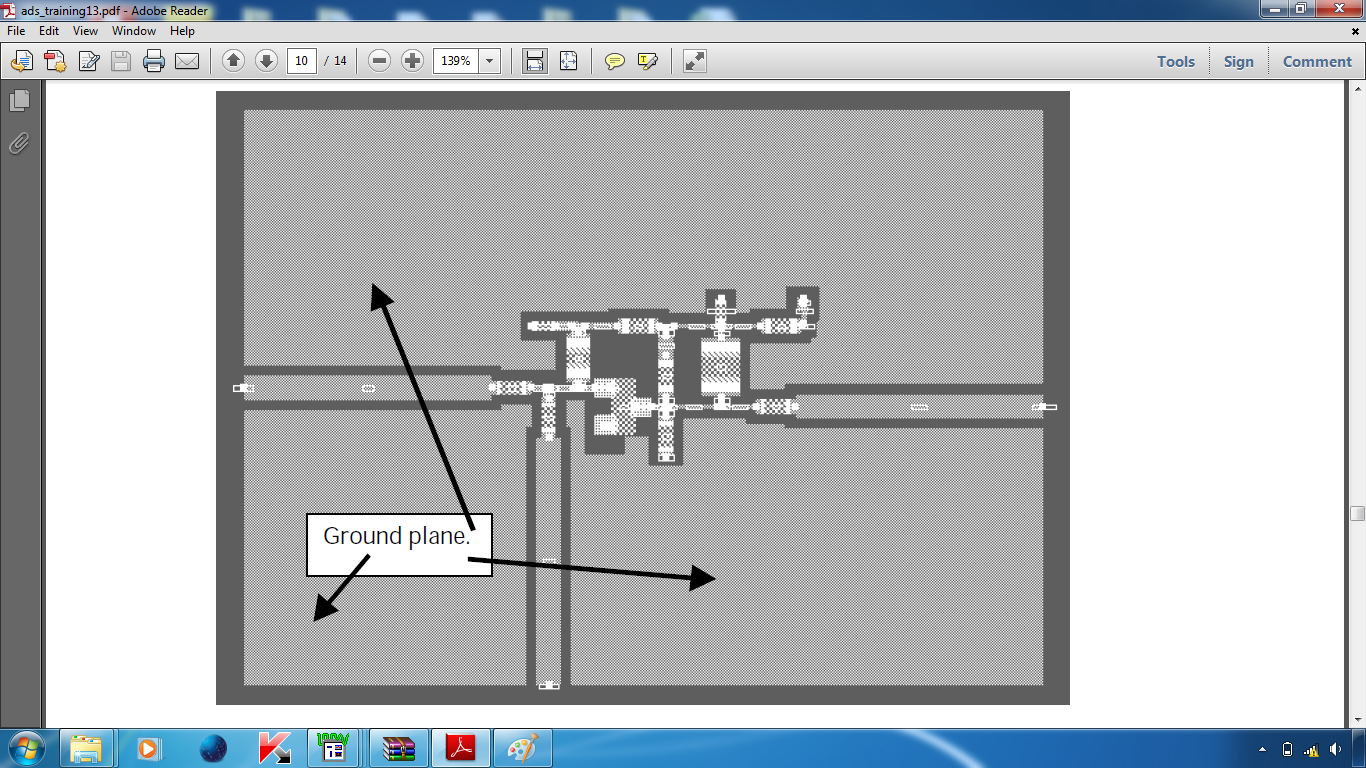
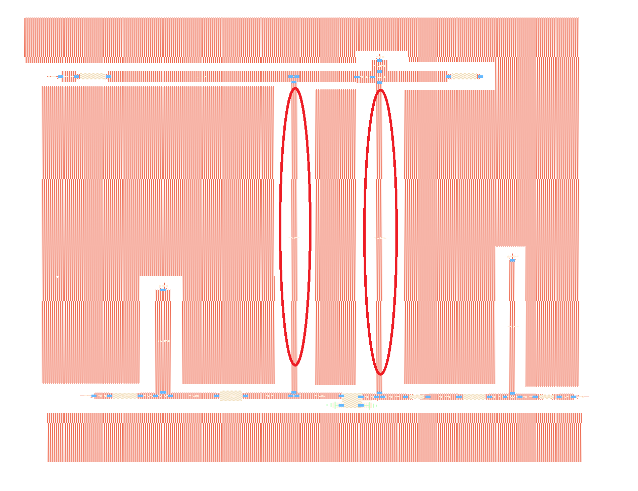
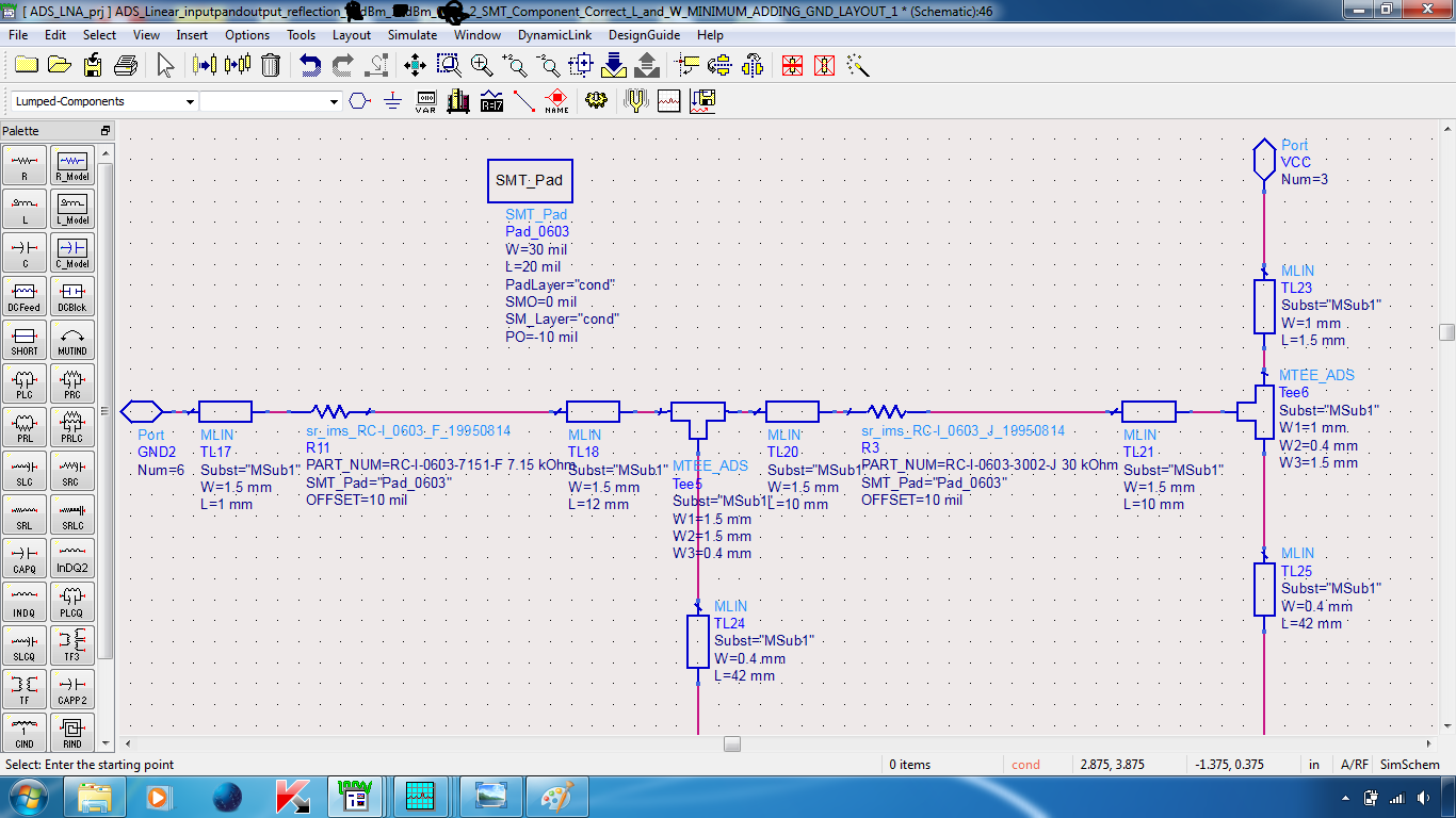
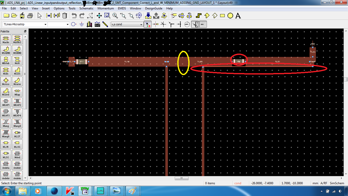
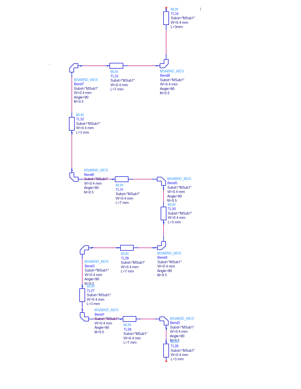
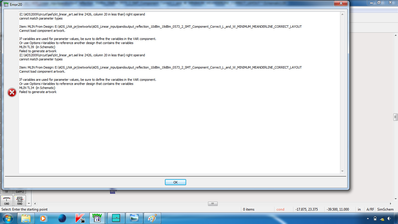
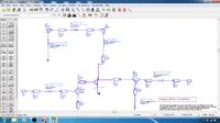
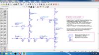
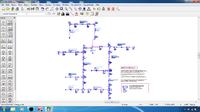
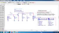
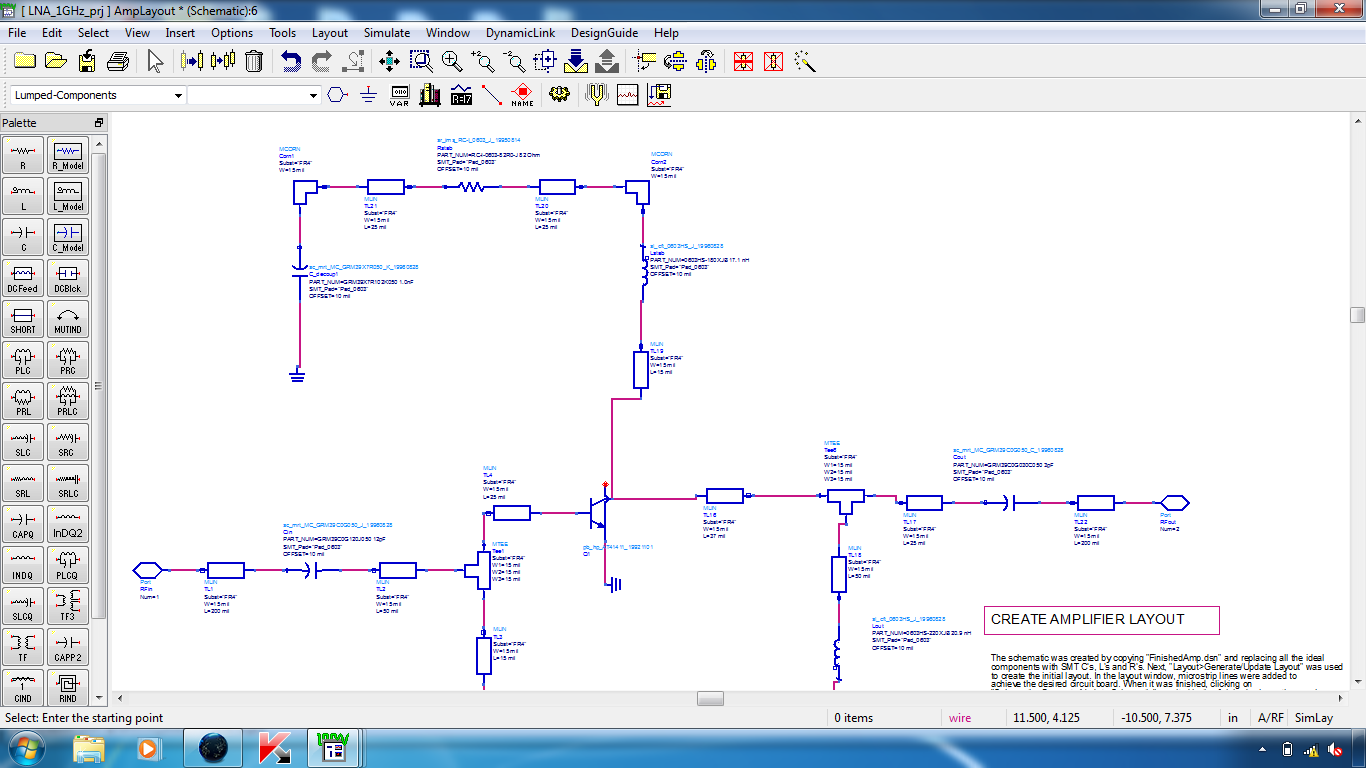
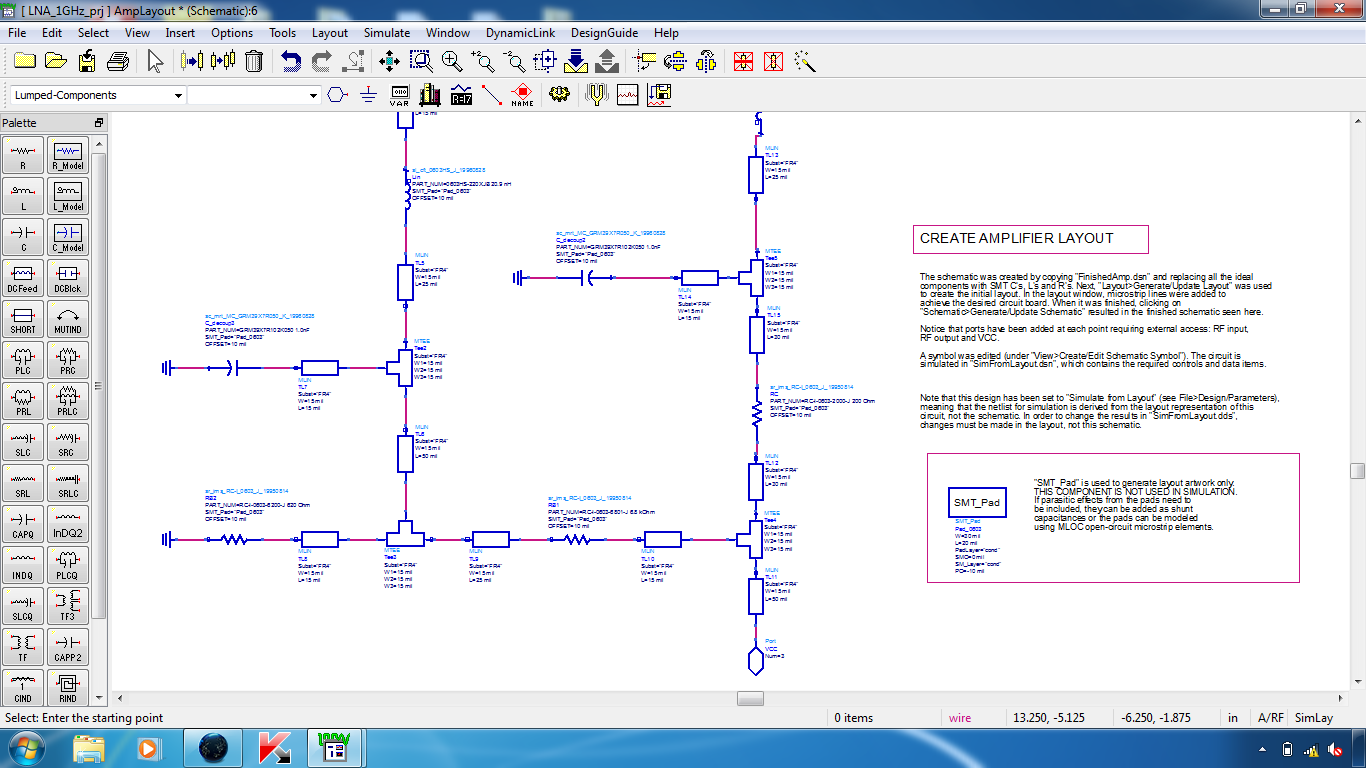
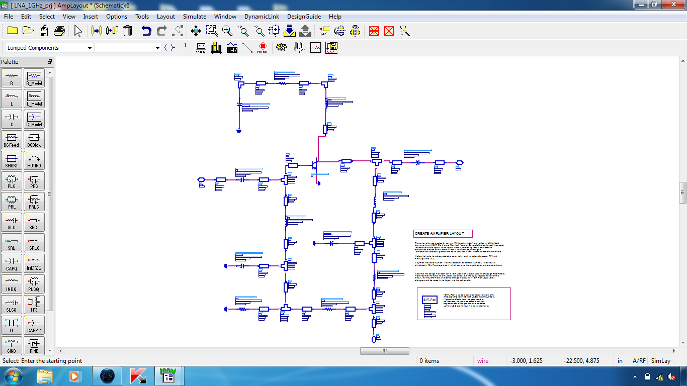
I am taking this example from C:\ADS2009\examples\MW_Ckts\LNA_1GHz_prj, have many doubt regarding on this Amplifier layout. I have attached .png files below (It is big ckt , I can't download it entire part it once, I made it part by part, first one is upper part, second one is lower part, third one is entire part, and fourth one is finished amplifier part)it is a 1GHz amplifier. I didn't understand the following points

(1) How they have converted the schematic finished amplifier into amplifier layout part.

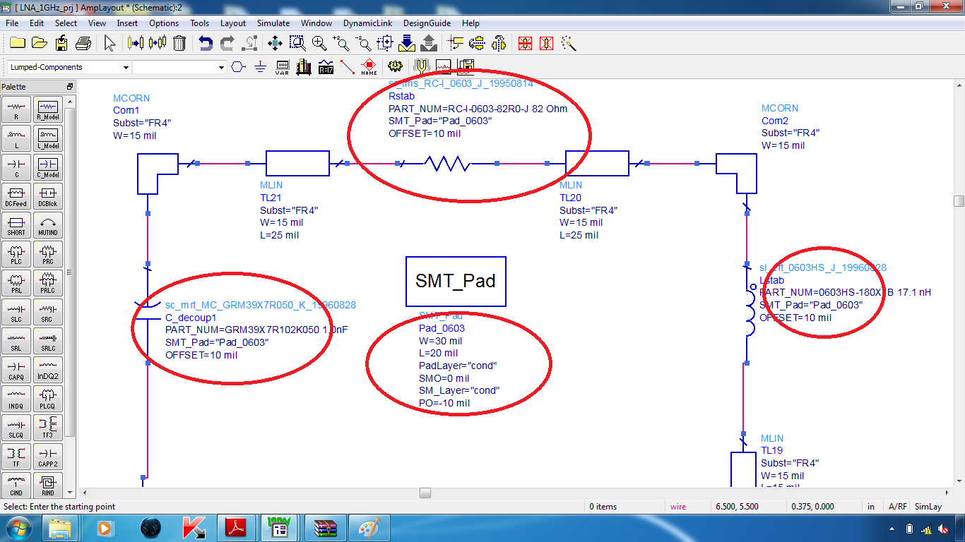
(2) You may notice in the amplifier layout , two microstrips lines connected between capacitor, inductor, resistor and MTEES. How they have calculated the values of MLIN's. Why we have to connect two microstrip lines between inductor , capacitor, resistor and MTEEs.

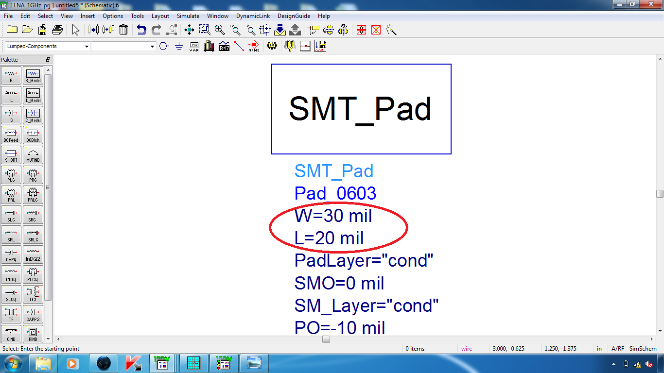
(3) Why they have used the SMT_Pad, how to define it.What is the use of SMT_Pad ?

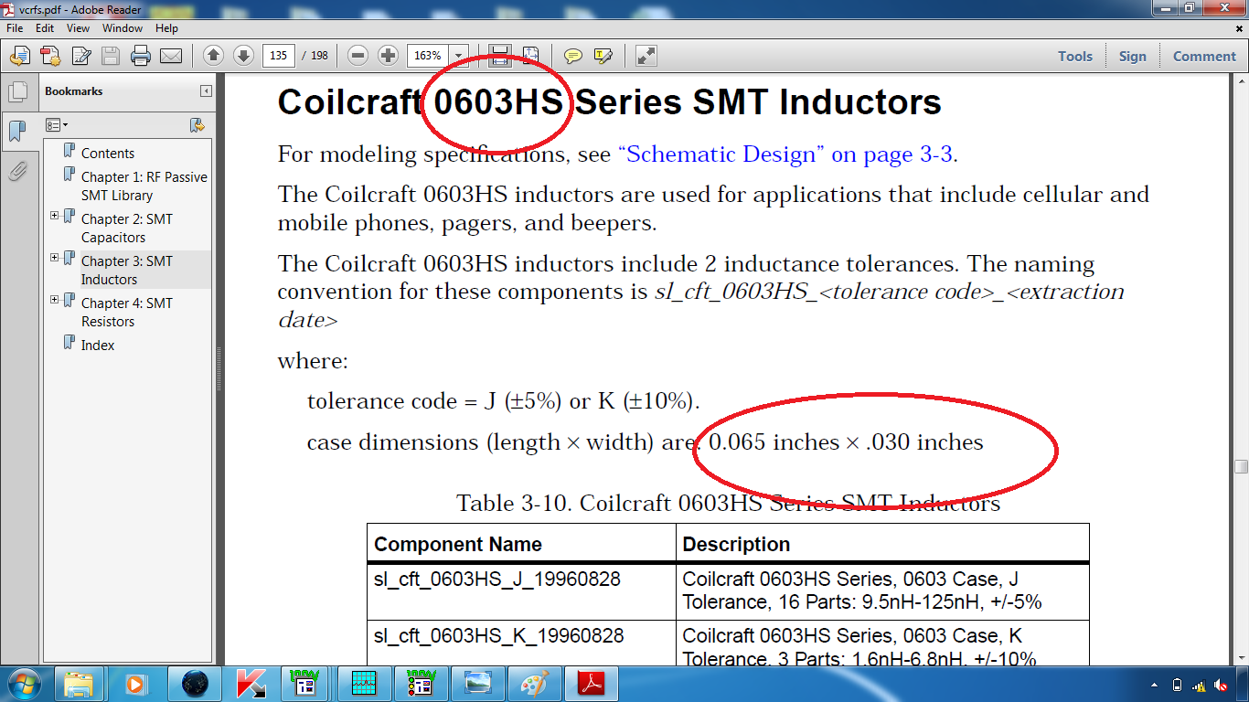
(4) You may also notice , they have used capacitors as sc_mrt_MC_GRM39X7R050_K_19960828, sc_mrt_MC_GR.............., indutor as sl_cft_0603HS.............., resistor as sr_ims_RC_I..................., . On What basis they have used these numbers and values, how we have to choose these SMT_Pad inductor, capacitor , and resistors.

(5) Somewhere they have used MCORN at the corner, some where they have left. Why they have not used MCORN, where ever corner is there.

(6) If we want to convert the schematic amplifier into layout , we have to convert it as like amplifier layout shown in the example and later press the Generate/Update Layout . Is it enough or some other parameter, we have to tune it.

(7) How we have to choose VCC and declare it.

The above doubts I have , anybody knows, can you help me to convert schematic into amplifier layout step by step as it was done in the example of ADS 2009 C:\ADS2009\examples\MW_Ckts\LNA_1GHz_prj . I have searched same topic in the EDABOARD, many have doubts on the above points.Please rectify it.


Last edited:

This looks like a very old design but you should read all the notes in each schematic and the A_Readme schematic as these explain how the author of this example developed the design.

1. The notes say it was created in the layout and then the schematic updated from the finished layout.
2. I see no case of two MLINs connected in series. There are many MLIN-MTEE-MLIN combinations. These would have been placed in layout to space parts out sufficiently.
3. The SMT_Pad creates the padstacks, in layout, that are used to attach the lumped SMT components, Chip Rs, Ls and Cs, to the board. It defines the size of each pad and the alignment with the chip and connecting traces.
4. The SMT part values are typically the closest available values to the original FinishedAmp component values but they may then have been optimized to adjust the response of the entire circuit to adjust for any offset resulting from adding the layout effects.
5. I do not see any corners in layout that do not have a MCORN/MTEE. A bend in the schematic does not necessarily mean there is a corner in the layout.
6. As answered earlier this final design was not generated from the schematic. It was drawn in the layout and then the schematic was generated from that. You can work either way if you wish but working directly in the layout is always quicker.
7. VCC is set in the SimFromLayout design.
 
RealAEL Sir,
In the SMT library, How we have to choose the values of SMT capacitor, inductor , and resistors. They are so many companies SMT capacitor, inductor and resistors are available.

(1) Suppose I want 40pF, 60pF , 100pF,0.1pF. If these values are available , it is o.k. If it is not available our desired value of capacitor ( suppose 40pF, I didn't find in the SMT library), what we have to do. If same value( 100pF) is available for different companies, which company value we need to choose. SMT library capacitor are available with different companies ( can be MURATE, Sprague, Microelectronics MPR7, AVx ......................). Suppose I choose 100pF from the MURATE company, remaining capacitors in the circuit, I need to choose the same company capacitor or we can choose any company capacitors.

(2) Suppose I want INDUCTOR and RESISTORS different values.If these values are available , it is o.k, if it is not available, what we have to do. What ever the points discussed in the (1) , I am facing the same problems with inductors and resistors as similar to capacitor problem.

(3) Similarly , What they have created and shown in the ADS2009 AMPLIFIER LAYOUT example. Can we similarly create layout for our own design (schematic)low noise amplifier as shown in the example AMPLIFIER LAYOUT?.


(4) Whatever we create layout for our own design as similar to AMPLIFIER LAYOUT example. For fabrication, do we need to change anything for the layout, will it work? or modification we need to do for our design.

(5) Equivalently schematic, we need to creating amplifier layout(we have to use equivalent values of SMT library values as similar values of schematic). How we have to cross verify, whether created layout correct or not?.


(6)For example, in MURATA capacitor vendor company, same value capacitor like 220 pF, 6pF ,12 pF , 0.5pF have appeared many times(sc_mrt_MC_...................). I am confused , which one I need to choose.

(7) You may notice in the example AMPLIFIER LAYOUT, they have used SMT_Library capacitors, inductors, resistors with the same series components Pad_0603. If one component is used same series, do we must follow the series the remaining components?.
 
Last edited:

1. & 2. The choice of which SMT part to use is entirely the choice of the designer. Any combination can be selected. In a 'real world' scenario though the designer may have little choice. The design may specify a 100pF capacitor but it then is the choice of the person buying the parts as to which to use. Usually the choice comes down to cost, which are the cheapest to purchase, and that could end up being any supplier. That choice may then change from one production run to another. Even when specifying a single supply source the performance from one batch to the next may change to some extent. The more accurate and consistant the performance the higher the cost.

The bottom line really is that the design should be robust enough to work with any device of a particular value, within the specified tolerance, from any manufacturer. Most times though the final decision in most cases is made on the basis of cost.

3. Of course it can be done. It would be a bit of work enabling layout representations of the devices but the SMT library would be a possible start for the passive parts. The transistor would then be the part that requires the most work. Then microstrip or PCB lines could be used to create the interconnects as required. This is how designers work with ADS all the time.

4. It should work if done correctly. There is no magic formula to say if you do it one way or another then it will work. It just takes good engineering to be successful. If it doesn't then that will mean it take more time to rework the design and add to the project costs.

5. There are things that can be done to simulate parts of the design from the layout using EM technology. The example design you have reference is simulated from the layout but that is really just netlisted from the layout so does not really simulate the layout effects that EM simulation would. These are only partial solutions though as there is no practical method of simulating the entire amplifier from the layout available today. No single simulation method exists only combinations of current methods that get close but not completely there.

- - - Updated - - -

6. You choose the one that is most appropriate. Yes, the same capacitance may be available in different chip capacitor series but each family groups different characteristics like case sizes, different voltages, different tolerance and different temperature ranges. You choose the one that best suite the application.

CompBrowser.png

7. No. You can use any that you want. Likely the choice would be constrained to certain tolerance or temperature range but there would be no requirement to make all parts the same type. Using similar case sizes may be better for automated manufacturing lines.
 
RealAEL Sir,
Thank you for your elaborate, knowledgeable,patience, and kind help for me.

Do you know sir?, which company RF passive SMT capacitors, inductors and resistors are commonly used, frequently, low cost(cheaper) as per your knowledge sir, can you tell me sir. Which must be available in all country sir.

I have shown one image below, whatever I have shown within the red ring, how to create that sub circuit symbol(Amplifier Layout X1), where it is available in the ADS2009. How get that the sub circuit Amplifier Layout X1 symbol.


In ADS you can create custom symbols for any design schematic.

Working with Symbols

You just need to be careful to create the correct number of symbol pins, the same as the number of ports in the schematic, and that the pin numbering is consistant with the schematic port numbering.
 
RealAEL Sir,
In the example AMPLIFIER layout , I have some following doubts.

(1) You may notice inductors and resistors SMT components , they have used 0603 series ( For example ,Inductor - sl _cft_0603HS_J_19960828, and Resistor-sr_ims_RC-0603_J_19950814)

(2) But , You may notice in capacitor SMT components, they have used other than 0603 series(For example, Capacitor- sc_mrt_MC_GRM39X7R050_K_19960828)

In inductors and resistors SMT components, they have used 0603 series , it is o.k, but capacitors they have used other than 0603 series. But in defining the SMT_PAD, they have taken only Pad_0603. They have not taken the capacitor series . Why they have not taken capacitor series into the account, while defining SMT_PAD.

(3) If we use different series SMT components inductor, capacitor, and resistor( with different series like, 0603,575,540,302,402,802). Do we require independently declare each series SMT_PAD definition for each component orelse for our convenience can we use all same series SMT components inductors, capacitors, and resistors ( as like in the example AMPLIFIER LAYOUT , they have used inductors and resistors same series components (0603), but capacitor other than 0603 series).

(4) You may notice, they have taken non linear transistor pb_hp_AT41411_19921101. What is my doubt is, do we not need any artwork transistor for creating layout. We must some width and length for creation of transistor. Is it sufficient pb_hp_AT41411_19921101? will it create itself artwork in the layout width and length?. If we use linear device , directly can we take linear transistor. For transistors, don't have like SMT components to create artwork (length and width).


1. & 2. Different manufacturers have different ways of creating their part numbers. Not all actually include the 0603 size literally in the name. The Murata GRM39 series devices are 0603. So all SMT devices are the same size.

3. You can use one SMT_Pad per individual device, one SMT_Pad for all SMT devices or any combination between the two. It does not matter the combination. The designer can choose whatever is appropriate.

4, The RF Transistor Library that the HP device is in is a collection of packaged BJTs, GaAs Fets and Power MOSFETs. As these are packaged devices the parts are provided with preconfigured layout representations, an SOT143 package for this particular device. The user does not need to do anything and they can be placed in the layout view. Other devices that are not preconfigured to include layout can have a layout representation added by the user if required. So you can take any device that does not have layout and add the appropriate layout view either using a predefined fixed layout or you can draw your own fixed layout. It is also possible to create scaleable artwork macros that scale to user-defined parameter values but that requires writing AEL code that is far beyond your current questions.

Schematic Capture & Layout > Artwork
 
RealAEL Sir,
How to measure impedance between two points in ADS2009.
 

This question has nothing to do with the listed topic. If you have a different question please start a new thread and clearly state the problem you wish to be answered. Do not bury it at the bottom of a totally unrelated topic. This is the only way that readers can see the new question and maybe provide an answer.
 
RealAEL Sir,
Sorry, I will make it new posting for that question. Below I have shown the two images, one is AMPLIFIER LAYOUT SMT_Pad and other is coilcraft 0603 HS series SMT inductors specifications. The following are my doubuts

(1) In AMPLIFIER layout example, they have taken all 0603 series inductors, capacitors and resistors. They have taken width and length of SMT_Pad as Width = 30mil, Length =20mil it is shown in the first image. What is my doubt is

(2) You may notice in the COILCRAFT 0603HS series , they have shown as case dimension as length and width (0.065 inches * 0.030 inches (65 mil * 30 mil)). But they have defined in the AMPLIFIER LAYOUT as width = 30 mil, length =20 mil. what is the permissible values of length and width of SMT_Pad defining.

(3) Can we take length and width above 65mil* 30mil or below 65mil * 30mil, or exactly 65mil* 30 mil. How we can choose the values of length and width of SMT_Pad definition.As we desire can we take length and width of SMT_Pad ?.


Last edited:

The SMT_Pad only draws the conductor under the end caps of the SMT device so the length of the SMT device is not important. Otherwise it does not matter exactly what size is used. The author of this example chose the domensions used. You can choose the dimensions that you think are best for what you want to do and what is best to manufacture the design. There are no fixed rules for all cases.
 
RealAEL Sir,
I have shown below image taking from the Example directory and open RF_Board directory and Mixer_Pager_Prj Example.I have the schematic and generated layout, want to go for fabrication of taking this layout. Before that I want to make layout for fabrication work.

(1) You may notice in the first image (Mixer_layout_Example),layout has ground plane,consisting of 3 areas, that is at least 10 mil away from all the components. I have shown red rings in the first image, want to remove that part. In example , they removed and showed. Similarly, I want to remove the red ring shown portion , also want remove the some portion of ground plane in between the components as shown in the example. Overall I want to remove the desired portion in between the components or somewhere in the ground plane.How to remove the desired portion in the ground plane, which option I need to use sir.

(2) I have shown the 2nd image, want to bend the MLIN's as like 2nd image shown. Which option I need to use in the ADS to bend MLIN as we desire.

(3) After completing the layout, I want to fabricate it. How I have to convert layout file into DXF and Gerber file . Why do we need DXF and GERBER file before giving fabrication.

(4) In layout view, if component parts are disassembled or somewhere, how to make them assemble ( snap together , we are using in AWR MWO) . Similarly which option I need to use in ADS for snap together all components.


- - - Updated - - -

RealAEL Sir,

(1) I have shown in below image mixer_layout_Example_1, I want to remove the shapes around the MLIN's also.

(2) I have shown the original image also. In that image removal portion , they have shown around all components. I want to remove the shapes between and around the all components as like original image.


Last edited:

1. and extra 1. and 2. Groundplanes are just polygons so you can simply draw 'freehand' the shapes you require using Insert > Shape > Polygon. You could also use the function Edit > Create Clearance but you would then need to manually add shapes to cover the spaces where you did not want the clearance. If that create clearance leave any unwanted separated shape then you can simply delete it.

2. MLINs are straight transmission line. You cannot bend an MLIN. If you want meandered lines then the most accurate method, without using EM, is to cascade the necessary MLIN and bend elements (MSABND, MCORN, MCURVE etc.) to get the shape you require.

3. That can only be answered by whoever is going to be manufacturing the board. You have to provide the data they required. The certainly may required gerber files to create the masks but may also need DXF data to define the mechanical information to make the board.

4. Why should the design get disassembled? If everything is being created correctly in the first place this should never happen. Find the step that is breaking the layout and don't do that step.
 
RealAEL Sir,
As you said. I followed it , got it .Thank you very much. But instead of polygon, I used rectangle and drawn the desired ground plane.

(1) As I discussed in the posting #13, I wanted to bend the MLIN, but it is not possible to bend MLIN. Because it straight transmission line. I have showed below the image with red ring. I used the MLIN length as 43mm, it occupies the most of the space in the board.If I reduce the MLIN length below 43mm , results will get disturb.Instead of MLIN, can we use something reduce the length ?, then we can save total occupying area. What we can use instead of MLIN to reduce the length?.


2. MLINs are straight transmission line. You cannot bend an MLIN. If you want meandered lines then the most accurate method, without using EM, is to cascade the necessary MLIN and bend elements (MSABND, MCORN, MCURVE etc.) to get the shape you require.

In this case I used MLINs and MSABNDs.

meander.png
 
RealAEL Sir,
What ever you have shown in your image, you have many MLIN's and using BENDS.You made it desired shape. But for my case (in posting #15), I have only one MLIN of length 43mm. But it can't bend as you have shown in the previous posting image( posting # 16). I want from single MLIN as you have shown like that I need to bend from single MLIN. How can achieve it from single MLIN of length 43 mm ?
 

You cannot do anything from a single MLIN except straight as you have shown. The trace I posted with the MLINs and MSABNDs has a total length of 43 mm so is equivalent to your straight single MLIN. Replace your single MLIN with the MLIN/MSABND style construction. You may need to tune the final lengths a bit to compensate for the effects of the bends but the same simulation results should be possible.

Once you have been doing layout a while AND you are using the latest version of ADS (ADS 2012/ADS 2013) there are other ways of doing this with traces and subnetwork wire models (although this still uses cascaded MLIN/MSABND element models) but that will not do what you want in ADS 2009. The method shown above is your most accurate option without using EM.
 
RealAEL Sir,
I am getting small error, while generating layout. I have shown below images schematic of amplifier and layout of amplifier. When I generated the layout , layout is not generated to similar to the schematic.

You may notice in the schematic R3 is in between TL20 and TL21, and also between TL24 and TL25.But when layout is generated, R3 is moved to the away from TL25. I have shown in the red ring.But it should be between TL24 and TL25. What should I do to bring the R3 in the yellow ring, I have showed in the Amp_Layout. Everything component in layout is coming correctly expect R3. R3 is moving away from the TL25. R3 is already in between TL20 and TL21, similarly it must between TL24 and TL25. What I have to make to bring the R3 in the yellow ring or in between TL24 and TL25 , and also between TL 20 and TL21. I have tried lot, couldn't get it.


RealAEL Sir,
I divided the 42mm MLIN , made it as meander line. But I am getting the errors, am feeling really difficult, can help me out difficulties. I attached the both images meander line and error message.


Status
Not open for further replies.

Part and Inventory Search

Welcome to EDABoard.com

Sponsor

Back
Top