Continue to Site

Welcome to EDAboard.com

Welcome to our site! EDAboard.com is an international Electronics Discussion Forum focused on EDA software, circuits, schematics, books, theory, papers, asic, pld, 8051, DSP, Network, RF, Analog Design, PCB, Service Manuals... and a whole lot more! To participate you need to register. Registration is free. Click here to register now.

low pass lc filter design

Status
Not open for further replies.
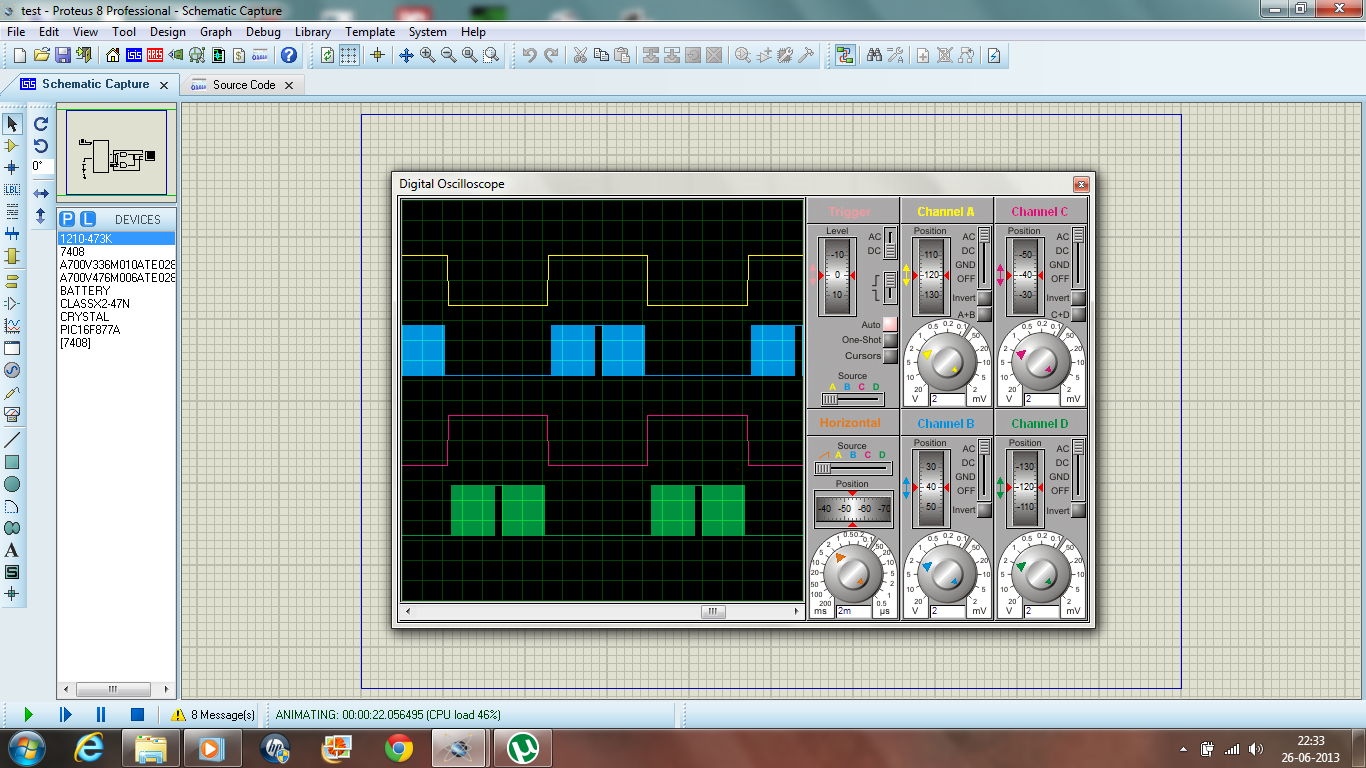
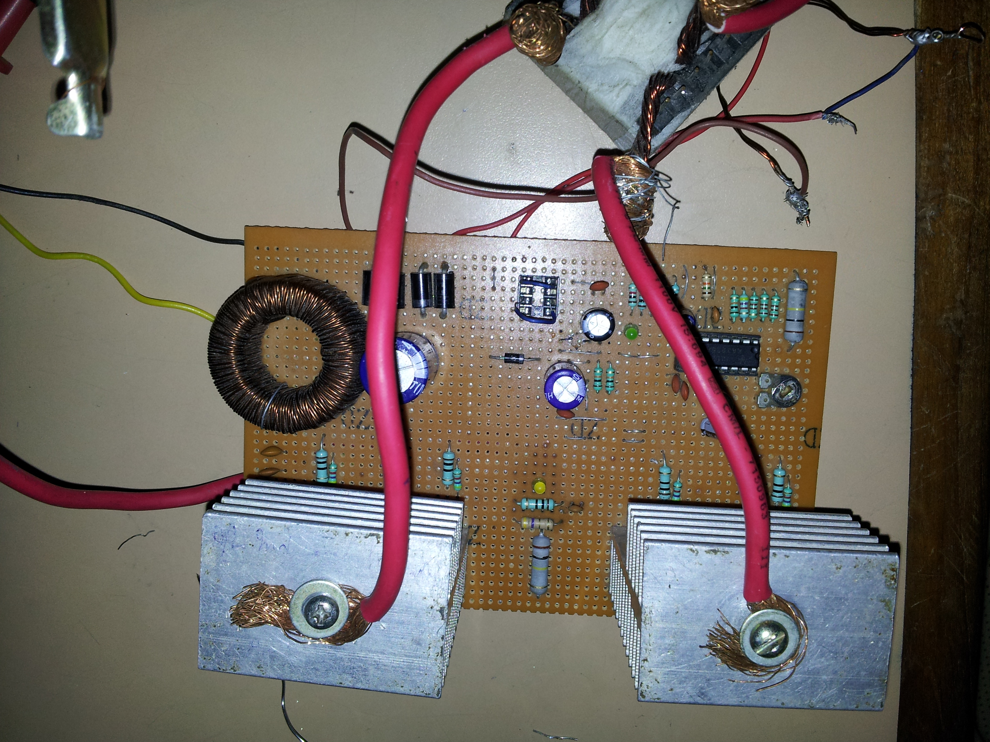
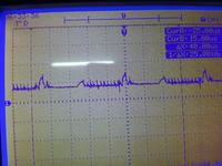
today i have tested my hbridge circuit again with low voltage (20v) and in output as i connected a resistive load ,i got the sine wave in oscciloscope.i am attaching the image below
https://obrazki.elektroda.pl/3578304900_1372178877.jpg
https://obrazki.elektroda.pl/6054555100_1372178880.jpg
i have tested my hbridge circuit with max dc bus voltage of 32v,

- - - Updated - - -

hii ,
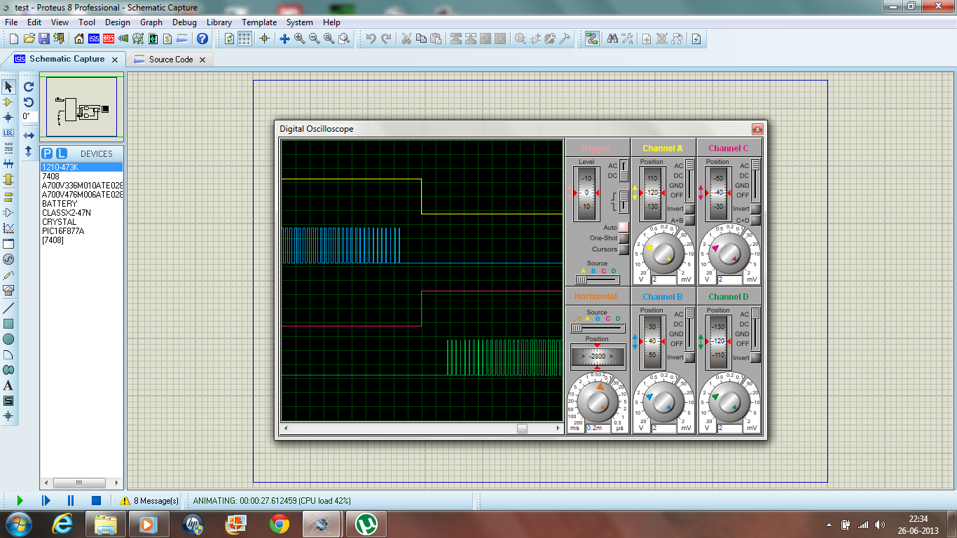
i have also seen my 311 v dc bus voltage on DSO, and it was like

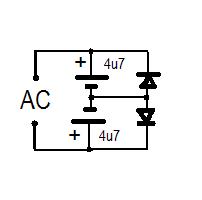
how to get pure dc , i have used an lc filter in output of the bridge rectifier , 3mh inductor and 47uf electrolytic capacitor,also i have added two 0.1uf ceramic capacitor in parallel to electrolytic capacitor,,, but there is ripple in output,,how to get a clean dc bus??

- - - Updated - - -

i dont have a dc source of 110v , i have dc source of 311v that my circuit is producing, tomorrow, i will check my hbridge with 311v dc, should i proceed with that? because ahsan is saying that ir2110 is not good for 311vdc bus,? what should i do now??

- - - Updated - - -

ahsan_i_h said:
In these pdfs one of the arms of H bridge is driven by 50Hz and other arm is driven by PWM signal.
But, perhaps, In your design top mosfets of the arms are getting 50Hz signal and bottom mosfets of the arms getting PWM
signal (but 10ms alternately). Is that right ?

If it is right, then your filter requires a minimum load current to work as expected.

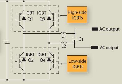
IN my design the high side mosfet of one arm hbridge is kept ON for 10ms,while in the same time ,the low side mosfet of other arm is getting a spwm signal.
and after adding a resisitive load i got the sine wave,.
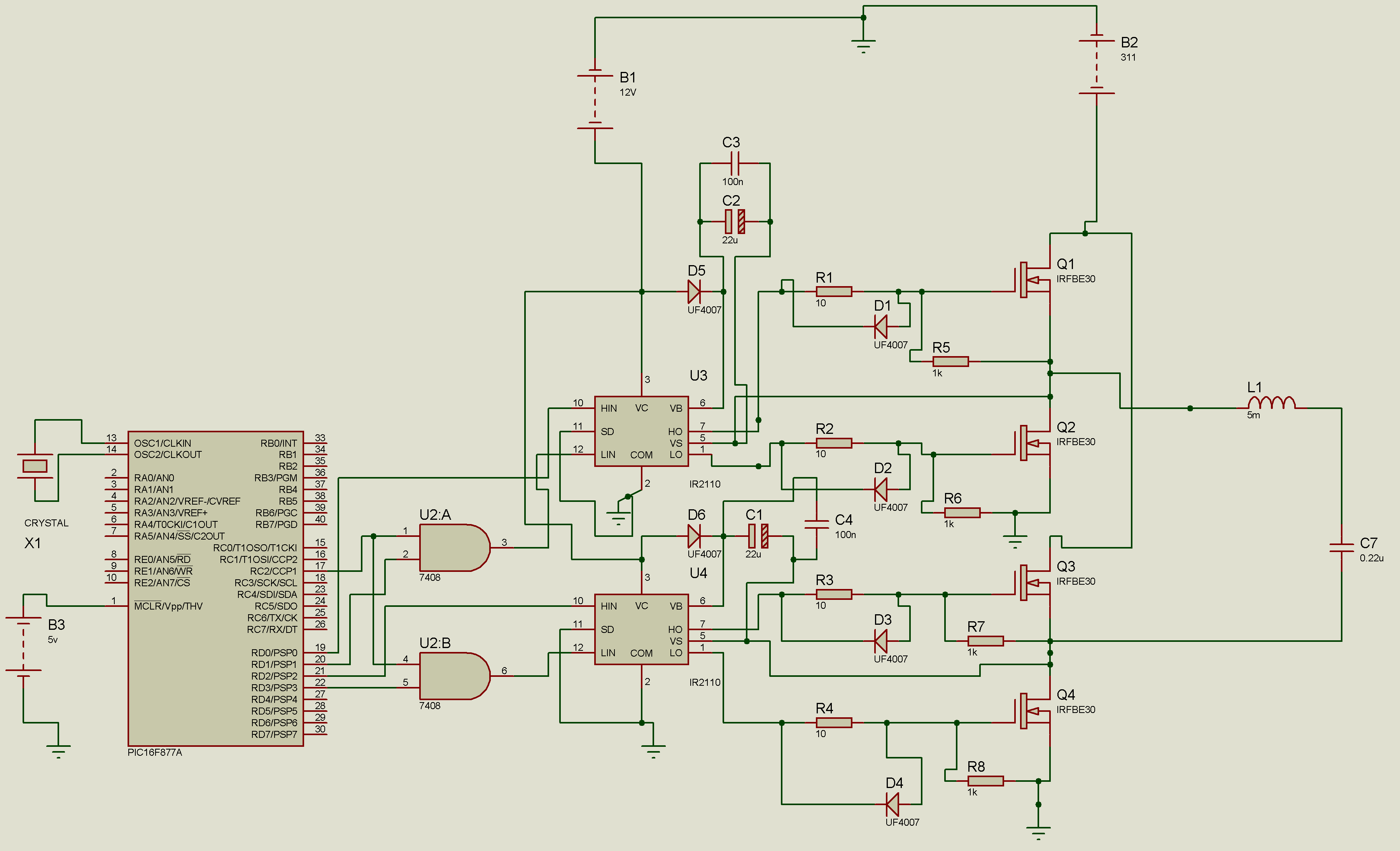
but should i test my circuit with 311v dc ?,, coz i have made my circuit 6 times,,and before filter ,it works gud,but as i connect the filter ,my mosfets blown out ,, earlier i was using torroidal core for inductor design ,but this time i am using ETD39 core with 1mm gap for my inductor as suggested by FvM,, i have made it to 5mh , and also used 0.22uf capacitor
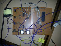
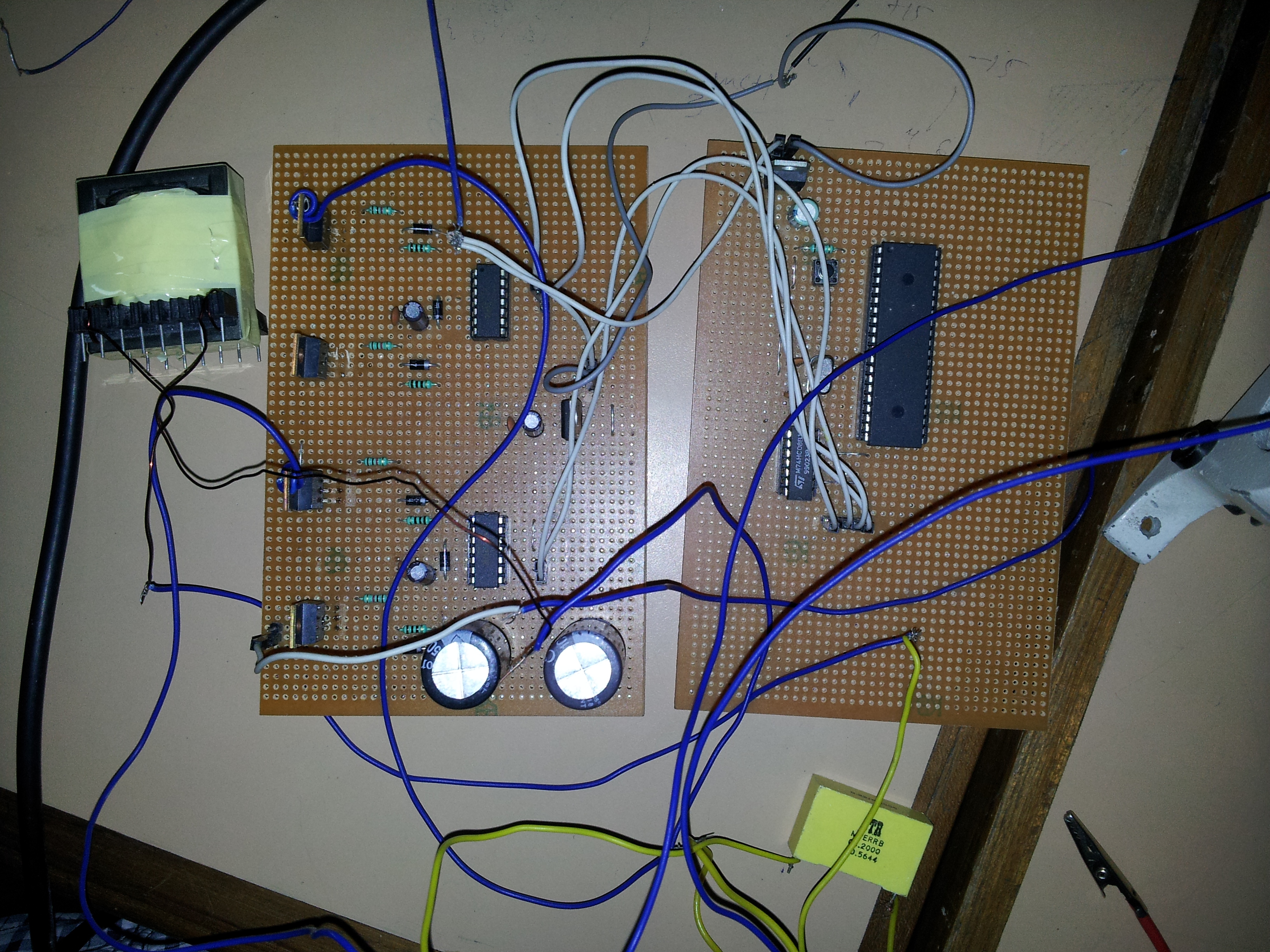
this is my circuit

so should i do high voltage test of my hbridge now? or make some changes?
 

my inductor as suggested by FvM,, i have made it to 5mh , and also used 0.22uf capacitor
I think you are still using elctrolytic capacitor in filter output which you are not mentioning and which is the killer.

i have used an lc filter in output of the bridge rectifier , 3mh inductor and 47uf electrolytic capacitor,also i have added two 0.1uf ceramic capacitor in parallel to electrolytic capacitor

If you have to use electrolytic capacitor, use it like in this configureation.

7242942500_1372188848.jpg


Don't use a big value like 47uF. It is passing very high currents at 311V, practically shorting output when polarity reverses and that's how, killing FETs is successfullly done.
 
Last edited:

I don't think that the filter uses an electrolytic capacitor, and there's absolute no need with 16 kHz PWM frequency. The text is ambiguous, but 47µF are most likely bus capacitors.
 

I don't think that the filter uses an electrolytic capacitor

It is mentioned in the very first post giving an indication. I seriously doubt it so.
Can we use electolytic capacitor to design a low pass lc filter for filtering spwm from h bridge ?
 

I am not using electrolytic capacitor for hbridge filtration. I am using 0.22uf box capacitor (non polarised) for hbridge filter.it can also be seen in the image that I hve uploaded (yellow color).
I have used two 100uf capacitor for dc bus 311v.
Should I connect my high voltage dc bus or make some changes before that??
 

Looking at the strip board setup in post #41, I imagine problems caused by parasitic circuit inductance and possibly insufficient bypasing. The shown waveforms, although not fully annotated with voltage ranges etc., look strange enough. There may be a problem of unintended parasitic switching by output stage to IR2110 inputs crosstalk. In this case, fatal damage of power transistor will easily occur, e.g. if output current or voltage exceeds a certain level.

Another point should be at least mentioned. The modulation method described in post #41 isn't able to handle four-quadrant operation, thus reactive output loads will distort the sine waveform when the output stage is in a passive quadrant (opposite sign of output voltage and current). To achieve clear PWM operation with reactive loads, you should use a four-quadrant capable modulation method, e.g. 3-level. Unfortunately, 4 independent PWM generator blocks are required for it in the µC.
 

hiii
this is my SPWM signal

and i have also provided dead time , it can be seen below

and this is my schematics


in this circuit , Q1 is kept ON for 10ms while Q4 is driven by SPWM, after 10ms Q3 is kept ON for 10ms and Q2 is driven by SPWM,,
carier frequency is 16khz,

at low voltage test i.e 32vdc , i am getting the sine wave of 22volts , which i have uploaded in #41,
but today i tested my circuit with dc bus voltage of 311, as i switched on my circuit , the output bulb (40watt) , glown for a instant ,and then my one side mosfet of hbridge blown out, where could be the fault in my design,, this was my 9th try,, please suggest me any solution.?
 
Last edited:

The drive waveforms and schematic are as I expected from post #41. The only unclear point is where the DC bus supply comes from, and what's the capacitance of bus capacitors that can be seen on the stripboard photo.

For the explanation of circuit failure, I would primary refer to my comment about wiring in post #46.

In addition, there's a problem that the bootstrap capacitors need to supply the high side driver for about 10 ms without recharging. According to the 1k gate-source resistors, the bootsrap voltage will fall from 12V to about 7V in this intervall, which is typically below Vb UVLO threshold, thus the high side driver must be expected to switch-off somewhere near the end of the halfwave. This shouldn't cause transistor damage, but is surely unwanted. Gate-source resistors should be considerably increased or completely omitted to avoid this problem.
 
What about the bypass capacitors? You need a tidy layout with small leads. Connect a 200 watts/220V bulb in series with Hbridge after DC bus filter capacitors during testing to avoid fets burning. Otherwise SPWM signal seems ok.
By the way, you have good camera in your SAMSUNG Galaxy S II, model GT-I9100 with software version I9100XXLSJ. Here you can upgrade
https://www.ibtimes.com/install-and...-i9100-using-aokp-custom-rom-tutorial-1105314
 

I hve made a separate circuit board for dc bus. My dc bus is regulated.this is my circuit


and I have used 0ne 47uf and two 100uf capacitor in parallel at dc bus. The two 100uf capacitor can be easily seen in my figure in post #41.

FvM said:
Looking at the strip board setup in post #41, I imagine problems caused by parasitic circuit inductance and possibly insufficient bypasing.
How to reduce parasitic circuit inductance ?
And what do u mean by insufficient bypassing?
 
Last edited:

How to reduce parasitic circuit inductance ?
We can't see the actual wiring on the stripboard bottom, so it's partly a guess. But shorter and wider traces or most likely required.

And what do u mean by insufficient bypassing?
I didn't see any VCC/COM bypass capcitors near the IR2110. By the way, there are no IR2110 Vss pins connected in the schematic.
 

FvM said:
I didn't see any VCC/COM bypass capcitors near the IR2110. By the way, there are no IR2110 Vss pins connected in the schematic
In my actual design I hve grounded the COM pin.
And didn't used any bypass capacitor at VCC I directly connected the VCC to 12v.

FvM said:
We can't see the actual wiring on the stripboard bottom, so it's partly a guess. But shorter and wider traces or most likely required.

At the back of the stripboard I have made the connections by melting soldering wire from one point to another. So there is no chance of loose connections.
Also my circuit is working fine at 32vdc bus ..m getting 22v at the output which is quite obvious. But the main problem is at high voltage test , my mosfet blows..if I don't attach the filter then mosfet dont blow .
As I attach the filter n switch on my circuit my mosfet get damaged..
 

It is good practice to connct a bypass capacitor loke 0.1uF between and +ve and -ve pins of every IC. It should be very close to IC pins. You can easily connect this capacitor on track side between pins on opposite side of IC. Further, there is no harm in putting a series bulb for testing to avoid damage as dscribed earlier.
 
but ALERTLINKS
what could be the possible reason of damaging of the mosfet as i switchon my circuit,?
is the reason is that i am not taking feedback loop from the hbridge to my first stage (dc dc ), ?
currently i am using feedback in my dc dc stage , so my 311vdc is regulated and constant,,
 

Even if IC is directly connected to +ve supply, it is required.
https://www.edaboard.com/threads/160554/

Gnerating DC_bus voltage and converting it to AC are seperate sections. If mains is rectified and filtered, you get the DC_bus for your experimentation. Treat them as seperate circuits. Both should worh OK indivisually. DC_bus sould be able to supply full load and regulate. This can be tested by using conecttig 220V bulbs because they are handy. If you dont put a small capacitor on mcu power pins, you get erratic operation. Do an experiment.

https://www.edn.com/electronics-blogs/bakers-best/4328787/Bypass-capacitors-no-black-magic-here
https://www.intersil.com/content/dam/Intersil/documents/an13/an1325.pdf
 
Last edited:
Ohk ALERTLINKS. I'll do that..
One more thing . Can u plzz check my filter design .
I hve used 5mh inductor , 0.22uf capacitor
Inverter rating is 220v 350 watts
Carier frequency is 16khz..
Plz check the filter values..are these values good or I need to work on it again??
 

In my actual design I hve grounded the COM pin.
I was asking about Vss pin.

One more comment about transistor damage. I was assuming that your design does unintended switching triggered by crosstalk to IR2110 input side, possibly causing a bridge short. But there are other possible explanations. The only practical way to find out is to continuously increase the bus voltage, e.g. with a variable transformer (don't know if your regulated bus supply would be able to achieve continuous variation or might be part of the problem by unexpected behaviour). While increasing the bus voltage, carefully watch circuit voltages and currents.

- - - Updated - - -

And additional thought how the problems might be related to reactant load currents.

If I understand right, you have used IRF740 (400V) and are now using IRFBE30 (800V). Both are MOSFET with standard (slow) body diode, indicated in the datasheet by a considerable reverse recovery time specification and particularly by a rather low reverse recovery dV/dt maximum rating.

According to your PWM scheme, inductive load will force the high side transistor's body diode to act as a freewheeling diode. During switch-on of the low side transistor, reverse recovery takes place, involving two possible problems:

- high diode current dI/dt and respective strong inductive voltage transients are generated in the output circuit. As said, they might crosstalk to the driver inputs.
- at worst case, exceeding of reverse recovery dV/dt causes an immediate latchup of the high side MOSFET (by triggering an internal parasitic PNP transistor)

The usual way to overcome this slow body diode problems is to increase the gate series resistor until the dV/dt rating is kept (e.g. up to 50 or 100 ohm)

Changing the PWM scheme to fully synchronous switching can mostly avoid body diode conduction if the PWM dead times are adjusted properly.
 
Last edited:
I hve used 5mh inductor , 0.22uf capacitor
Why invent the wheel again? There are many application notes online for inverters, UPSs like IRF and microchip and other sites. There mostly inductors are used in both output legs ranging between 0.7-1.2 mH AND 2.2uF to 4.7uF filter capacitor. Of course these valued depends upon voltage, frequency, output power. For 240V, 16-20KHz, 300-600 watts, the values fall in this range.
8844171800_1372666740.jpg


Althoug single inductor is also used.
 
Last edited:

Symmetrical filter design brings some EMI advantages, but is unlikely the problem in the present case.
 

  • Like
Reactions: --BawA-- and FvM

    FvM

    Points: 2
    Helpful Answer Positive Rating

    --BawA--

    Points: 2
    Helpful Answer Positive Rating
Status
Not open for further replies.

Similar threads

Part and Inventory Search

Welcome to EDABoard.com

Sponsor

Back
Top