Continue to Site

Welcome to EDAboard.com

Welcome to our site! EDAboard.com is an international Electronics Discussion Forum focused on EDA software, circuits, schematics, books, theory, papers, asic, pld, 8051, DSP, Network, RF, Analog Design, PCB, Service Manuals... and a whole lot more! To participate you need to register. Registration is free. Click here to register now.

modified sine wave smps inverter

Status
Not open for further replies.

--BawA--

Advanced Member level 1
Joined
Nov 28, 2012
Messages
479
Helped
43
Reputation
86
Reaction score
42
Trophy points
1,318
Location
Noida, INDIA
Activity points
4,926
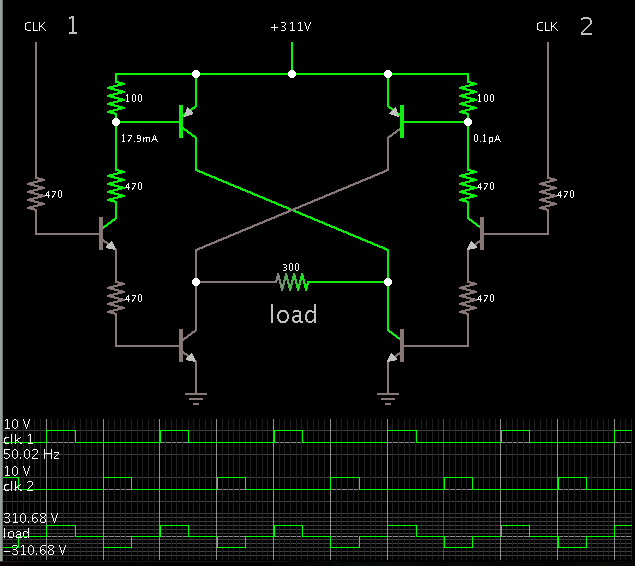
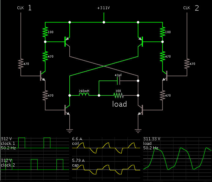
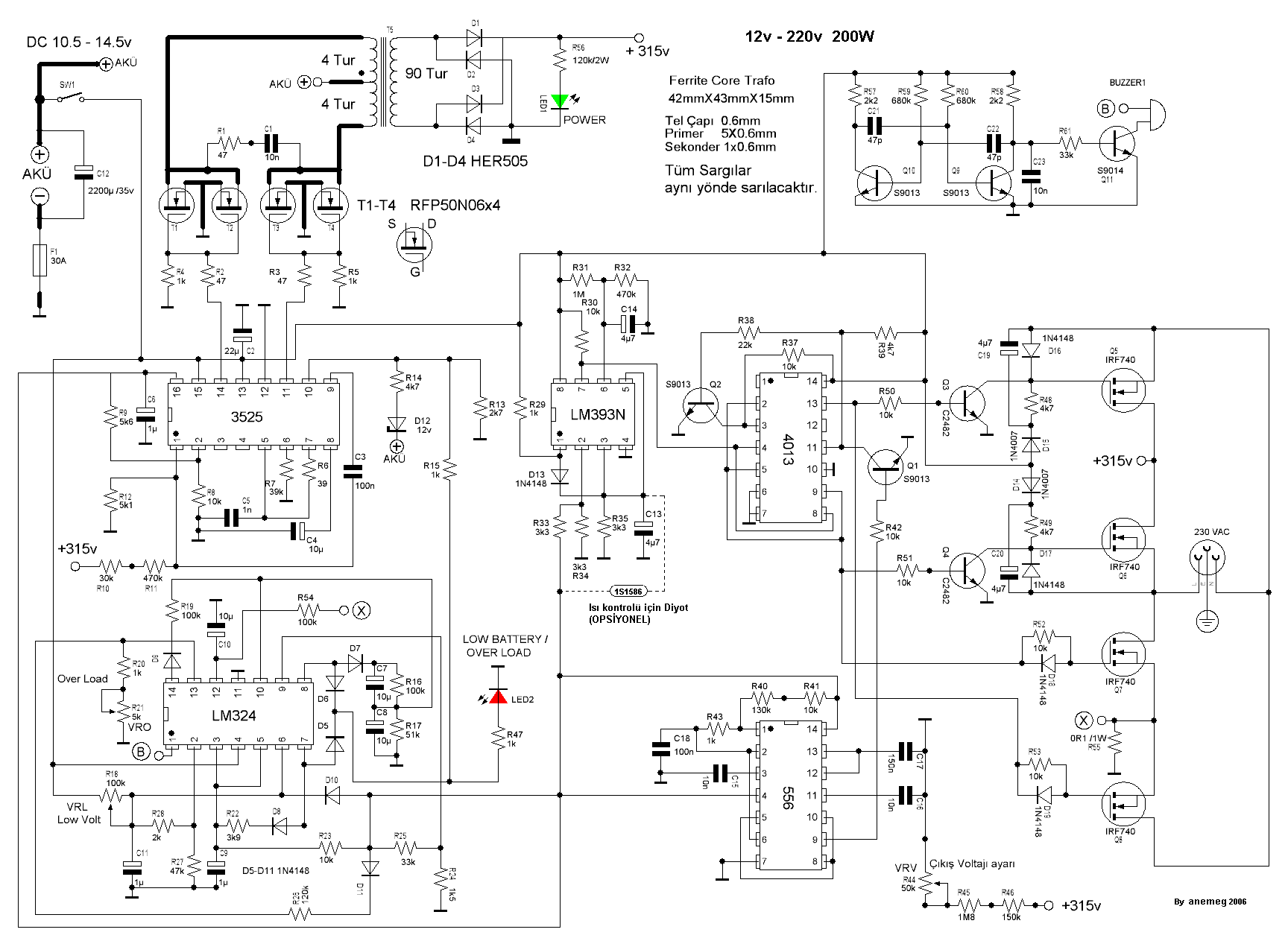
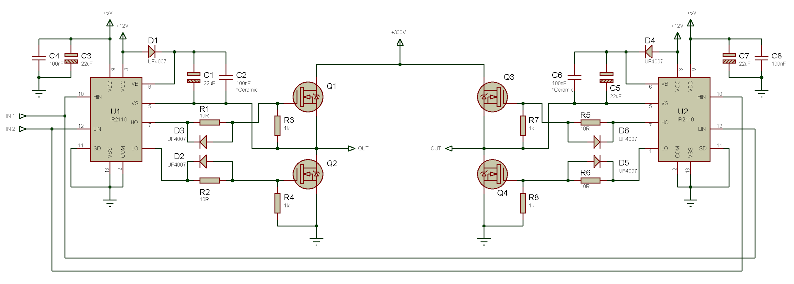
I have generated 311vdc from 12vdc, now my aim is to convert this dc bus into modified sine wave with the help of full bridge and sg3525 ic ..please tell me how to proceed..I have also made full bridge circuit ..so how to drive the 4inputs of full bridge from sg3525 in order to get modified sine wave at the output.
 

This method appears to work in simulation.

It allows low-volt control signals to be compatible with the high voltage supply.


To produce a modified sine wave, the two control signals are 25% duty cycle, staggered 180 degrees.

None of the bias network resistors has to carry more than 20 mA.

The wires cross above the load, so as to allow a less congested wiring layout.
 

Please let me know about Transistors and Resistors values of your inverter?
 

My schematic is to illustrate the concept.

The mosfets/transistors should be selected to endure the maximum voltage/current they will be exposed to. (Rather, make it 2X the maximum, to give a safety margin.)

The resistor values need to be low enough to provide sufficient bias current to transistors. But high enough so they do not permit more than is necessary. Notice that you need to pay attention to the amount of current that might flow out of the PNP bias down into the NPN bias.

IRF740 mosfets are popular N-type.
For the P-type it is suitable to use one with about the same V and A rating.

My schematic does not show the devices used to generate the clock signals. To do that will require an independent circuit.
 
how to connect LC filter?

This suggests you now want a sinewave output, rather than your original specification for a modified sine wave.

If you wish to add an LC filter, it is better to apply it to AC square waves rather than modified sine waves.

With a modified sine wave, the mosfets/transistors are off during part of the cycle. You cannot use a series LC arrangement.

You can arrange the coil and cap as a second order filter.

Screenshot:

 
It is Falstad's interactive animated simulator. A free download at falstad.com/circuit.

The link below will open his website, load my schematic above, and run it on your computer:

https://tinyurl.com/kl95lft

You can alter values. Right-click on a component, and select Edit.

You can save a circuit. Click File, select Export. A text window appears. Copy the text and paste it into a word processor. Save the document.
 
Dear BradtheRad,

Please let me know can I use any NPN Power Transistor of center four transistor?
 

Dear kabeer02,

Did you make this circuit at post# 14 ,did this works well ?
 

you can drive the mosfets using two ir2110 or using gate transformer.
 
Assalamoalaikum Hamid,

Please let me know if you can make any inverter,if yes, please tell me its power rating.
 

Status
Not open for further replies.

Part and Inventory Search

Welcome to EDABoard.com

Sponsor

Back
Top