Continue to Site

Welcome to EDAboard.com

Welcome to our site! EDAboard.com is an international Electronics Discussion Forum focused on EDA software, circuits, schematics, books, theory, papers, asic, pld, 8051, DSP, Network, RF, Analog Design, PCB, Service Manuals... and a whole lot more! To participate you need to register. Registration is free. Click here to register now.

[SOLVED] Linear Tech Current sense application circuit - need some clarification

Status
Not open for further replies.

thunderdantheman

Member level 4
Joined
Jan 19, 2010
Messages
74
Helped
13
Reputation
26
Reaction score
15
Trophy points
1,288
Location
Australia
Activity points
2,111
G'day,

I'm trying to build a high speed high-side current sense amplifier and while searching out possible candidate op-amps I came across the LT6016/LT6017. The datasheet http://cds.linear.com/docs/en/datasheet/60167fa.pdf shows an application circuit of a high side current monitor with a FET output... (I've included the circuit below) now I can't work out how or why it works.. i'm probably missing something really simple but i'm rather stumped atm! any one care to explain it's operation?

Isense.PNG
 

now I can't work out how or why it works..
You didn't tell which point is unclear to you. I can imagine two possible issues:

- How does said "over-the-top" mode of LT6016 work. I fear the simplified internal circuit misses some details, we simply have to believe that the specified parameters are achieved. A pnp current mirror with the emitters as + and - inputs can do the job in principle.

- Presuming the previous point is right, you might have problems to understand the feedback concept. But it's basically simple and can be found similarly in other high-side current-sense amplifiers. Just assume that the current through the FET creates a voltage drop across the 200 ohm resistor that cancels the shunt voltage so that the amplifier differential input voltage is zero.
 
Ahhh... the feedback is what i didn't quite grasp... so its a cheeky way of achieving negative feedback... i see. so what is the advantage of this method over configuring a traditional diff amp setup? is it faster? ive never come across such a circuit. still strugling to write its equation...

- - - Updated - - -

Ahhh... the feedback is what i didn't quite grasp... so its a cheeky way of achieving negative feedback... i see. so what is the advantage of this method over configuring a traditional diff amp setup? is it faster? ive never come across such a circuit. still strugling to write its equation...
 

Indeed, this is a commonly used circuit; the same fundamental idea is used for pretty much all high-side current sense amplifiers.

The op-amp will output whatever it must to make its inputs equal. As current flows through the load and a voltage starts to appear across the sense resistor, the op-amp gets upset and its output rises. The output will rise until the op-amp is satisfied—when its inputs are equal. This occurs when the same voltage that appeared across the sense resistor now appears across the top 200Ω resistor (i.e., the voltages cancel and the op-amp is left with zero volts across its input). Voltage appears across the 200Ω resistor when current flows through it, and that current must flow through the 2kΩ resistor beneath the MOSFET. Since the currents are equal, the voltage across the 2kΩ resistor is 10x bigger than the voltage across the 200Ω resistor, and voilà we have a gain of 10x and a level-shift to ground level.

In this explanation, I didn't even consider the fact that the op-amp has current flowing into its inputs. As shown on page 17 of the datasheet, we see that when the inputs go "over-the-top," the input stage becomes a common-base stage with 14µA flowing into each input (according to the EC table on page 3). When this 14µA current flows through a 200Ω resistor, it causes a 2.8mV offset. To compensate, equal 200Ω resistors are placed at both inputs. The same offset is thus added to both inputs, so they cancel out.

- - - Updated - - -

thunderdantheman said:
so what is the advantage of this method over configuring a traditional diff amp setup?

A diff amp has high sensitivity to component mismatch. Especially when you're measuring a small voltage, you'll want very well-matched resistors. This circuit will yield good accuracy without requiring super-duper resistors. I also wouldn't be surprised if there's a speed advantage.
 
Awesome! thanks for that guys! understand the concept now and since found a number of high-side current monitor ICs that use that exact circuit, it is indeed common! However... they're all quite slow... 1us response time is as quick as I can find. Even if i were to construct the application circuit... the specified op-amp only has a slew rate of 0.45V/us ... add the response time for the FET and the 1us prepackaged device is looking good! Poor slew and GBW must some of the trade offs for having greater than Vcc common mode inputs. Doesn't help me keep a mosfet within the SOA from a short circuit on a low impedance supply though.
 

Apart from bandwidth limitation of the involved components, you should be aware of limited common mode rejection at higher frequency. In most cases, the common mode rejection ratio will be the limiting factor of galvanically coupled high side sensing amplifiers. You can expect a certain improvement by making the structure strictly symmetrical, including the current feedback. But for higher speed, optical or magnetical coupled sensing circuits should be considered.
 
Depending on how much accuracy you need, there are other options...

For example, you can build your own current sense amp out of discretes.

This circuit seems reasonably fast:

csa2.png

If you want more accuracy there are tricks that can be played, but if you just want speed and simplicity this might work for you.
 
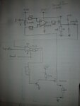
Thanks again guys.... I've learnt a lot! That's a neat little circuit too ZekeR... i'll be sure to tuck that one away. Infact I might even breadboard it this weekend and have a play. For the time being though, I've decided to add a voltage double to my design to utilize NMOS devices... rather than having a charge pump to drive each gate, a single 22V rail which I can then run an LT1215 off and keep within the CM input range without killing CMRR too much (nice pint FvM) - only a few hundred uV error. It has 50V/uV slew rate so i'll have response times in the tens of nano seconds. the output will feed my ADC for current monitoring and also an LT1016 ultra-fast comparator with latch to latch the NMOS channel off in the case of an over current event. There's probably no need for the 20R resistor on the -ve input as just looking at that resistor would probably generate more voltage across it than the bias currents in this device! The NMOS device I'm using has quite large Qg so for once I can use it to my advantage as a soft start for the load through the gate pull up resistor...

IMG_20130531_163525.jpg
 

Status
Not open for further replies.

Similar threads

Part and Inventory Search

Welcome to EDABoard.com

Sponsor

Back
Top