Fabien
Full Member level 1
Good morning everyone,
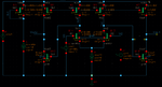
I'd'like to design a simple fully differential OTA for a switched capacitor integrator. As it needs to be very low power, I'm wondering how to start the design and how to fixe the W and L of the transistors? The design I made doen't have the common mode in the middle range (Vdd/2).
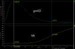
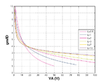
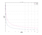
I read some papers about the Gm/ID methodology, but as the best case is in moderate inversion, I'm wondering how to achieve this requirements. What is a typical procedure to design an OpAmp?
Can anyone help me how to start a design?
Thank you
I'd'like to design a simple fully differential OTA for a switched capacitor integrator. As it needs to be very low power, I'm wondering how to start the design and how to fixe the W and L of the transistors? The design I made doen't have the common mode in the middle range (Vdd/2).
I read some papers about the Gm/ID methodology, but as the best case is in moderate inversion, I'm wondering how to achieve this requirements. What is a typical procedure to design an OpAmp?
Can anyone help me how to start a design?
Thank you