Continue to Site

Welcome to EDAboard.com

Welcome to our site! EDAboard.com is an international Electronics Discussion Forum focused on EDA software, circuits, schematics, books, theory, papers, asic, pld, 8051, DSP, Network, RF, Analog Design, PCB, Service Manuals... and a whole lot more! To participate you need to register. Registration is free. Click here to register now.

Help need for drawing IIP3 and P1dB using AWR MICROWAVE OFFICE.

Status
Not open for further replies.
You are doing so many things WRONG here that I am not sure where to start.

Overall you do not seem to understand the difference between a linear and nonlinear model. The bias ALWAYS has to be applied to the nonlinear model directly. You cannot simulate a model without bias and then reuse that simulated data with the bias and expect it to work correctly. You should not be using the S2P symbol with the .ds data as the non-linear model. The .ds file is linear data because it was generated with an s-parameter simulation. Use the symbol original Avago model, ATF54143_dt.dsn, directly in the schematic.

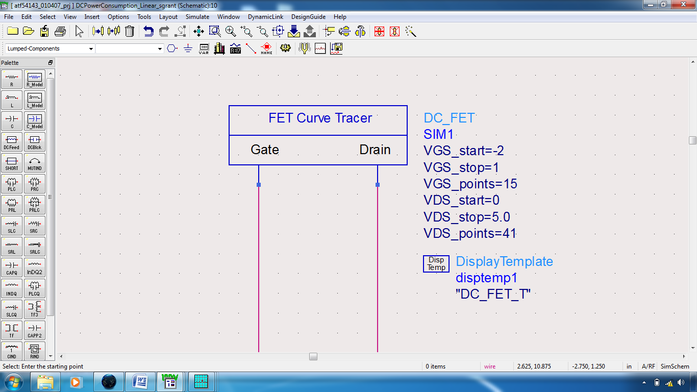
To evaluate the DC Bias of the device I would include this in a curve tracer schematic template ane simulate it there to determine the correct operating point.

The 31 Ohm resistor in the drain connection is totally wrong. I have never see and design built like that. Any change in current would change the drain voltage and alter the device performance. You should NEVER have resistors in series in that part of the amplifier. Why use a 5V DC source and simply throw away 2V in the resistor. Using a 3V DC source directly with no resistor should give a better Vdc operation.

A series 1600 pF capacitor in the input matching circuit does not seem right either. you would have many problems finding such a device that works correctly at 1.3GHz.

Before you start looking at the device in operation though you need to re-examine your design. Make sure that when you look at ONLY the input matching network with the bias network and ONLY the output matching network with the bias networks and do separate 2 port s-parameter simulations on each that you get the correct reflection coefficients (S22 for the input matching network and S11 for the output matching network) are as you requir for the design. Until that is correct the design will not work.

LNA_match.png

Schematic #1 af541433b_lineardevicemodel.dsn

1. The af541433b_dt_3_terminal.ds data is linear data at (at the wrong bias) so using this model is not correct.
2. You cannot do a DC simulation using a linear data model and get realistic answers.
3. The s-parameter simulation does not consider terminal voltages in the cirsuit so the DC source do not need to be there. They can be removed and replaced by grounds, they are effectively short circuit for s-parameter simulations or they could be annotated as "deactivated and shorted" or set to 0V. The important part is that the remainder of the biasing network should be included.

Schematic #2 54143_Original_EDABOARD_1.dsn

1. You cannot do a DC simulation using a linear data model and get realistic answers.
2. Same comments about the DC voltages source as in Schematic #1 above.

Schematic #3 af541433b_lineardevicemodel_withoutbias.dsn

1. The af541433b_dt_3_terminal.ds data is linear data at (at the wrong bias) so using this model is not correct.

Schematic #4 af541433b_dt_3_terminal.dsn

1. You are doing an s-parameter simulation of the circuit without the necessary bias. Reusing the model this way will never work. Take out the Term symbols and put back the original Ports (4 of them). Then use the symbol for this design file in the schematic for your design directly. This is the only way that this model should be used.
2. Even as is this device will not perform correctly as you have a disconnected wire for Term 3. You should never have red pin, red indicated a disconnected part.

Your design should end up looking something like this for linear s-parameter simulation:

LNA.png

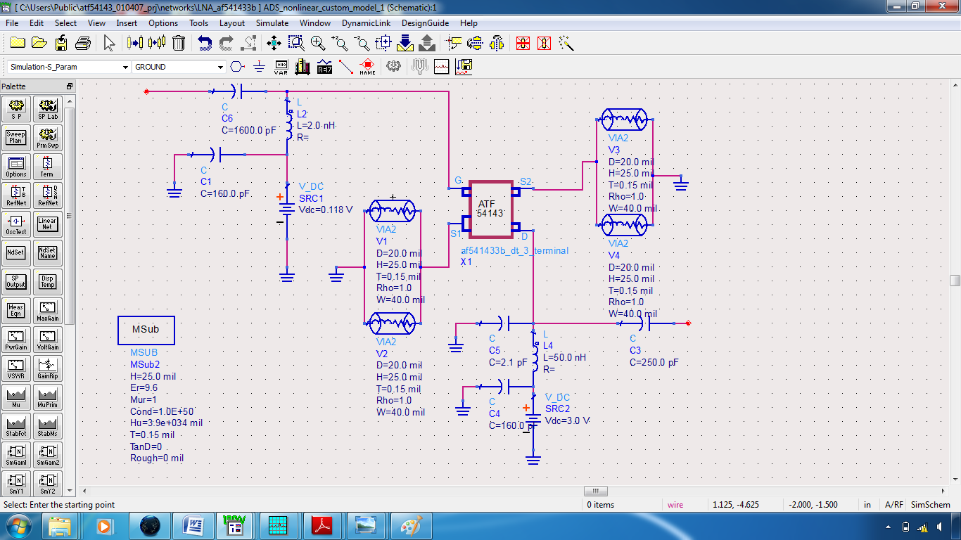
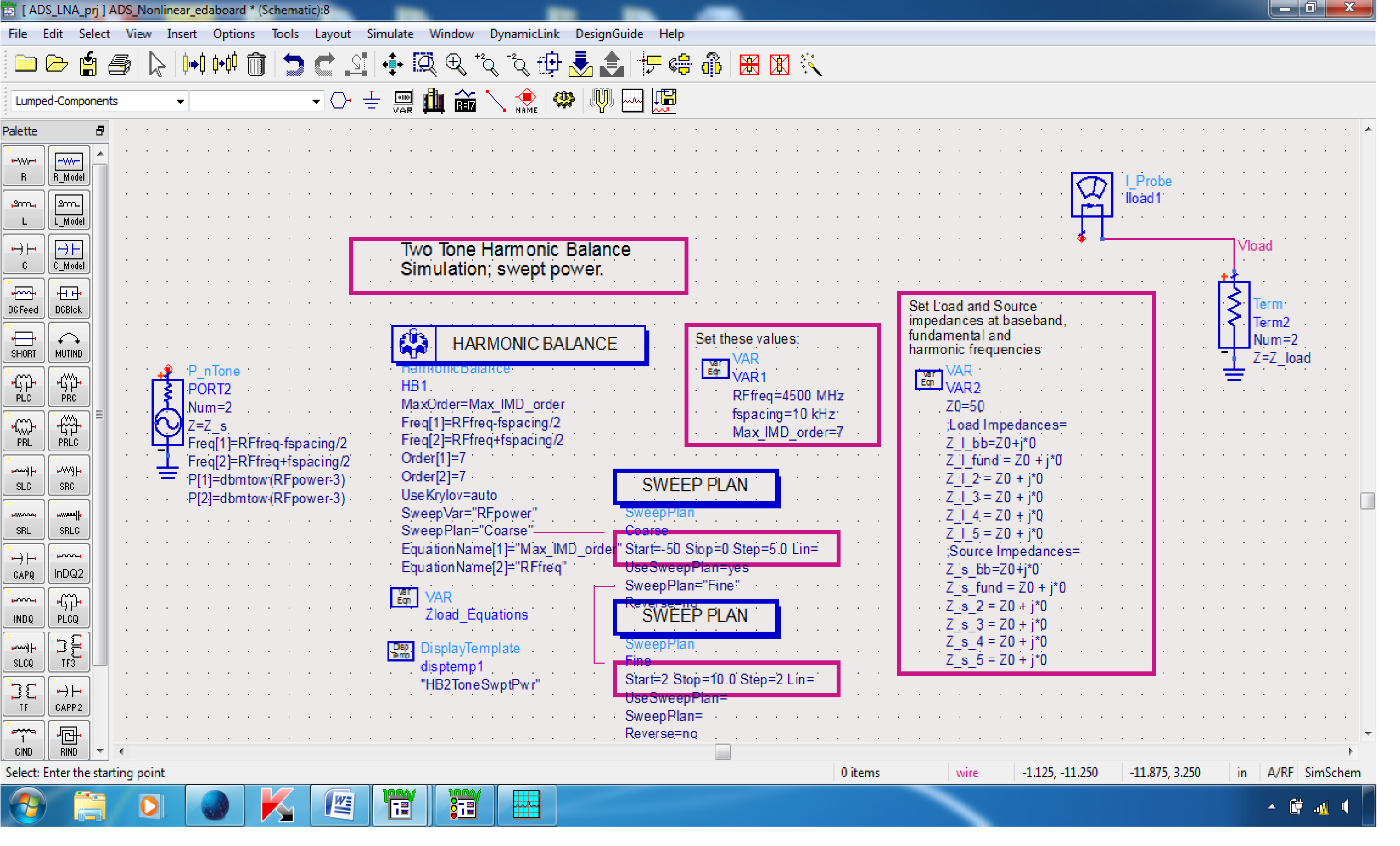
and for non-linear simulation:

LNA_NL.png

Basically if you are using the af541433b_dt.dsn model downloaded from the Avago website and in any schematic that is used to simulate any circuit using that model if you do not see the same symbol for the packaged device then you are not doing it correctly.
 
Last edited:
RealAEL Sir,
I am really confused , accept it that I have made so many mistakes. I am really confused where to start. ADS nonlinear device model is there, we have to use the custom symbol for using ADS nonlinear device, where is the custom symbol in the ADS2009, how I have to access it. I have searched in the palette, couldn't find it.Once I get the custom symbol then I need to connect input and output matching and biasing , later I have to simulate and compare results with the linear model results. Please tell me, how to use the nonlinear model using custom symbol.
 
This is by far the easiest question you have asked so far. This is one of the basic operating modes of ADS. The custom symbol, when it is defined, is used whenever you the design itself is used in any design heirarchy. There are three easy ways to re-use any design but unfortunately one of them is not the palette.

Either of the following methods will work:

1. Open both the ADS main window and the schematic window where you wish to re-use design together. In the main window find the ATF54143_dt design in the "Project View" list. Now simply click and drag the design into the schematic window (keeping the mouse button held down). Click on the required location in the schematic window to place the symbol.
2. In the schematic window open the Component Library List. It is a button on the second toolbar that looks like a set of books or the menu command Insert > Component > Component Library... In the resulting window select the Projects line in the left panel. Again find the ATF54143_dt component in the right panel and click and drag it to the schematic window.
3. In the schematic window in the Component History toolbar dropdown list, the second one on the second toolbar next to the Palette selector list, simply type in the name ATF54143_dt and press enter. Again click the location in the schematic window where you wish to place the symbol.

Wire up the rmainder of the design and all is done.
 
RealAEL Sir,
I followed as you said , got the custom symbol creation. It helped me lot. Now I connected the custom symbol to input and output matching and biasing circuit,tried to simulate it to notice s-parameters (S11,S21, S22, S21) and stability.But it is not allowed to simulate, simulation option is disabled ( i.e. F7) . What I have to do to get simulation option enable.


If the simulate button are not active then that means that there is currently no license available to run the simulator. Please check from the ADS main window Tools > License Information... and then in the Usage tab make sure that the expected licenses are available and not in use by another user/program session. The problem is nothing to do with the design/schematic itself.
 
RealAEL Sir,
Other schematic , it is active. But # 24 schematic only , it is not active. I went Tools> License Information > usage, it is showing that No licenses usage information available
 

If there is another schematic window open and simulation is active there maybe it is holding the license. Go to that schematic window and run Simulate > Stop and Release Simulator... Then reopen the problem schematic window.

If that does not work you may need to restart ADS.
 
RealAEL Sir,
All other schematic simulations are active, but this is only not active. I did run simulate and stop and release simulator and reopen schematic window and also restarted ADS also . Simulation button is inactive only.

- - - Updated - - -

RealAEL Sir,
All other schematic simulations are active, but this is only not active. I did run simulate and stop and release simulator and reopen schematic window and also restarted ADS also . Simulation button is inactive only.
 

I think I see what you have done. It looks like you have used Windows Explorer to create a folder in the networks directory of the atf541423_01047_prj called LNA_af541433b and copied or saved the design ADS_nonlinear_custom_model_1.dsn into that folder. You cannot do that. All design files must be directly in the networks folder. Copy everything out of the LNA_af541433b folder up to the network directory and remove the empty folder. When you open the design in the correct location then it should work.

FYI - You can create 'folders' from within the main window to organize the designs as required but these are virtual folders for display in the ADS main window only. The design files themselves are still in the project networks folder.
 
RealAEL Sir,
Other schematic , it is active. But # 24 schematic only , it is not active. I went Tools> License Information > usage, it is showing that No licenses usage information available

Buddy..
I can not see any simulator block on your schematic.Tell me where it is ??
 

Buddy..
I can not see any simulator block on your schematic.Tell me where it is ??

That would certainly give an error if the Simulate button was available to run but that is not the issue with the btv_murthy's schematic. The simulation controller and other pieces being missing will not cause the toolbar button to become non-operational. It should be active all the time.
 
RealAEL Sir,
What happend you know, posting #24 , simulator button is active , when file is in the untitled. When file is saved with some name, that simulator button is inactive. I have simulated that untitled file itself . For S-parameters , It was showing S11 and S22 reflection coefficients.But S21 and S12 is showing as invalid. Whatever I have shown the custom model and input and output matching and biasing is it correct.

- - - Updated - - -

RealAEL Sir,
What happend you know, posting #24 , simulator button is active , when file is in the untitled. When file is saved with some name, that simulator button is inactive. I have simulated that untitled file itself . For S-parameters , It was showing S11 and S22 reflection coefficients.But S21 and S12 is showing as invalid. Whatever I have shown the custom model and input and output matching and biasing is it correct.
 

When you create a new schematic design ADS always gives it the name untitled until you define a suitable name. At this point the design is only held in memory so ADS knows how to handle this and it works correctly. It appears though that when you do the step of saving the design and assigning your own name it is getting save to somewhere other that the correct networks folder and that is causing the simulate button to become deactivated.

When you us the file Save Design or Save Design As... try the following:

SaveAs.png

Check the top of this window and make sure that it show the networks subdirectory of the current project as the directory where the design is to be saved. If it does not navigate to the correct folder before saving the design. Use the Browse Folder button to open that view in the window if necessary.

Only ever save designs directly into the networks folder of the project you have open.
 
RealAEL Sir,
Now it is working , as you said I made it. What was the error, it was showing HIDE FOLDERS instead of showing BROWSE FOLDER. I made it as BROWSE FOLDER instead of HIDE FOLDER as you have shown,it is working nicely. Now clearly Simulation button is active. Thank you very much for your patience help.
 

RealAEL Sir,
Now I measured IIP3 and OIP3 and P1dB Compression for the nonlinear device model using ADS template HB2ToneSwptPwr for IIP3 and OIP3 measurement and ADS template HB1ToneSwptPwr for measuring 1dB compression point. For DC power consumption, I used the template FET_CURVE_TRACER for linear device model used.

My doubts are as follows

(1) I set RFpower = 0dBm(1mW) , how to check p1 dB compression point obtained value HB1 Tone SwptPwr graph shown below, how to check IIP3 and OIP3 values for the graphs using HB2 Tone SwptPwr for nonlinear device at 1.3GHz.How to cross verify these obtained values. how we can make confirm obtained values are correct or not.

(2) I used FET_CURVE_TRACE template for measuring dc power consumption for linear device model. I obtained 150mWatts,how to cross verify this value whether it is correct or not. For group delay variation , I used linear device model and enabled group delay in the S-parameters and obtained 3.05E-10 as group delay value. How to cross verify this obtained group delay value is correct or not.

(3) Which equation I need to use for calculating FIGURE OF MERIT of lna or which template I need to use for calculating FOM.

(4) I set the RFpower = 0 dBm (1mW), obtained p1 dB compression as -2.025 , IIP3= 8.592 and 8.603 (lower and higher IIP3), OIP3 = 24.60 and 24.61 (lower and higher OIP3), these points may notice in the IIP3 and OIP3 measurement .png figure. Suppose if I change the RFpower = -10dBm, these p1 dB compression, IIP3 and OIP3 may also change, we can say that we need to notice IIP3, OIP3 ,and P1 dB for 0dBm RFpower for our case. How much power we need to substitute for RFpower in terms mW or microwatts. Which IIP3 and OIP3 I need to notice, weather lower or higher IIP3 or OIP3.

(5) If IIP3 comes more than 0dBm, can we say that LNA is linear.


Last edited:

WOW! I cannot believe you are asking some of these questions. Your really do not appreciate what these measurements are or understand what they mean. Many of you statements are totally incorrect.

(5) If IIP3 comes more than 0dBm, can we say that LNA is linear.

Absolutely not. Whether an amplifier can be described as a linear device or not is a function of how it is being operated and not derived from some arbitrary measured or simulated data point. An amplifier is operating in a linear (uncompressed) mode if and only if the output power changes by 1dB for each and every 1dB increase in input power, i.e. the gain is constant with respect to input power level. If the input power level is increased to a point that the output power increases by less than 1dB for every 1dB increase in input power then the amplifier in exhibiting gain compression or saturation and is therefore not operating in a linear mode. Linearity is a function of the performance of the amplifier under specified operating conditions. Therefore the same amplifier can be operating in a linear model sometimes and nonlinear at other times.

(1) I set RFpower = 0dBm(1mW) , how to check p1 dB compression point obtained value HB1 Tone SwptPwr graph shown below, how to check IIP3 and OIP3 values for the graphs using HB2 Tone SwptPwr for nonlinear device at 1.3GHz.How to cross verify these obtained values. how we can make confirm obtained values are correct or not.

Again this is wrong. The 1dB compression point of an amplifier is an attribute of the device that is usually measure using swept input power. It cannot be evaluated at a single input power level like at RFpower = 0dB. Both the IIP3 and OIP3 measurements are also an attibute of the amplifier that are evaluated based on swept input power measurements typically but the measurement can be derived from a single power point provided it is a point in the linear performance range of the amplifier. Using swept power simulation is a vital method used to validate the measurement. In this case RFpower = 0dB is too large to accurately predict these measurements.

You are correct that the P1dB compression point is derived from the HB1ToneSwptPwr template and the IP3 measurements are derived from the HB2ToneSwptPwr template but as it clearly says on both these displays the moveable markers, m3 on the 1 tone display and m1 on the 2 tone display, adjust the output spectrum plots and have nothing to do with any other measurements.

(2) I used FET_CURVE_TRACE template for measuring dc power consumption for linear device model. I obtained 150mWatts,how to cross verify this value whether it is correct or not. For group delay variation , I used linear device model and enabled group delay in the S-parameters and obtained 3.05E-10 as group delay value. How to cross verify this obtained group delay value is correct or not.

Wrong again. You cannot measure power consumption using the linear device model. S-parameter data files typically do not contain any DC data to accurately perform DC analysis, especially swept DC analysis that is used for the curve tracer templates. The simulator will attempt to extrapolate from the lowest AC frequency point in the data file, 100MHz for the files in this case. This will never give accurate enough data. The only thing that you can be confident of is that if the data was measured at Vds=3V and Ids=60mA that equates to 180mW of delivered DC power to the Drain pin of the device. You must be using the nonlinear model for the transistor to perform any fixed or swept DC analysis.

(3) Which equation I need to use for calculating FIGURE OF MERIT of lna or which template I need to use for calculating FOM.

There is no template available in ADS to measure Figure of Merit. You need to write your own equations in the ADS Data Display to do this.

(4) I set the RFpower = 0 dBm (1mW), obtained p1 dB compression as -2.025 , IIP3= 8.592 and 8.603 (lower and higher IIP3), OIP3 = 24.60 and 24.61 (lower and higher OIP3), these points may notice in the IIP3 and OIP3 measurement .png figure. Suppose if I change the RFpower = -10dBm, these p1 dB compression, IIP3 and OIP3 may also change, we can say that we need to notice IIP3, OIP3 ,and P1 dB for 0dBm RFpower for our case. How much power we need to substitute for RFpower in terms mW or microwatts. Which IIP3 and OIP3 I need to notice, weather lower or higher IIP3 or OIP3.

Now this is the part where everything is totally wrong. All P1dB and IP3 (input and output) are totally independant of input power. If you are trying to evaluate either of these measurements for a specific power level then you are most likely interpreting the data incorrectly.

If we start by looking at the P1dB measurement. This is the operating point of the amplifier where the power gain is compressed by 1dB compared to the linear gain of the amplifier, usually expressed as the input drive power level that gives 1dB of gain compression. The -2.025 figure you are quoting is the actual gain compression for 0dBm input power. This is not the 1dB compression measurement. Both the sets of graphs you provided have tables that show Power Gain and Gain Compression/Reduction. What you should see is that for lower input power levels the gain is constant at just over 18dB. While the gain is at this constant value this is your linear region of operation. As the input power increases at some point the gain starts to decrease and the gain compression/reduction increases as the input power is increased further. The input power level where the gain is compressed by 1dB to 17dB is you P1dB compression point. This appears to be somewhere between the inpout power levels of -5dBm and 0dBm. you will need to simulate this power sweep at a few more points to more precisely determine the actual value. Once the power gain drops below the 18dB level then you are operating the amplifier compressed and it is no longer operating in a linear mode, it is becoming saturated.

The IP3 measurements also needs to be computed when the amplifier is not saturating, in linear mode. Again the IP3 measurement results for the amplifier is independant of input power. Any intercept point measurement is computed by simple geometry extrapolating from a power level measurement at the fundamental frequency and another at the 3rd order intermodulation tone for an input power that causes the amplifier to be in a linear mode of operation. This can be any power level. It just has to be one that does not drive the amplifier into compression. Under this mode of operation the slopes of the Pout/Pin curves for the fundamental and 3rd order tone are constant, slopes of 1 and 3 respectively, and the math is still valid. If the input power is too high and the amplifier is compressing these slope assumptions are not longer valid and the math will generate the wrong results. As was stated previously your statement about these measurements for 0dBm input are above the point where compress occurs so those values of IIP3 of 8.592dBm and 8.603dBm and OIP3 of 24.60dBm and 24.61dBm are not correct. This is why it is really good to do these a swept power measurements. If you look at your tables that show IIP3 (Input TOI) and OIP3 (Output TOI) you will see they start at the lowewr power point as being constant values with IIP3 of 14.44dBm and 14.42dBm and OIP3 of 32.47dBm and 32.45dBm. These are the correct values. These values stay the same as the input power is increased until the amplifier starts to saturate and the slope assumptiong for the Pout/Pin curve start to fail. As you may also see the input and output values differ by 18dB which is the linear gain so that aligns with other data. The slight difference from low to high side in both cases are due to the difference in gain of the amplifier between the two frequencies injected into the circuit to do this measurement but this different is a couple 1/100th dB so can really be ignored.
 
RealAEL Sir,
Everything is working fine. But when I connected the HB2 Tone swept power for measurement of IIP3. I took the HB2 TONE SWEPT POWER from the INSERT> TEMPLATE and connected this template to the our LNA and changed only our frequency, I didn't change anything. When I press the simulation button,it was showing simulation failed. It was showing the so many things, these things I have shown in the below images. After showing the so many things, it is showing the correct IIP3 and OIP3 results. How to avoid this simulation failed for '0' power, '1' power, '2' power etc ............ How to avoid these messages after simulation button pressing. Even it is showing these messages, it will show proper results. Can we ignore these messages?. If we don't ignore, how to avoid this


This is part of the normal operation of Harmonic Balance simulation. The simulator will automatically adjust the power level as required to achieve convergence. It may be possible to avoid this by adding extra points to the power sweep. Try Start=-50 Stop=-10 Step=5 for Course Sweep Plan and Start=-9 Stop=10 Step=1 for Fine Sweep Plan.
 
This is part of the normal operation of Harmonic Balance simulation. The simulator will automatically adjust the power level as required to achieve convergence. It may be possible to avoid this by adding extra points to the power sweep. Try Start=-50 Stop=-10 Step=5 for Course Sweep Plan and Start=-9 Stop=10 Step=1 for Fine Sweep Plan.

RealAEL Sir,
Thank you very much for your help, it is working nicely. It is avoided, what it was showing earlier. Now it is simulating in a usual way. Thank you for help.
 

RealAEL Sir,
For single stage low noise amplifier, whatever you told the sweeping plan (i.e. try Start= -50, Stop= -10 Step =5 for Course Sweep Plan and Start =-9, Stop =10 Step =1 for Fine Sweep Plan), I used it and got the very early results without any much time and no failure errors. But the same LNA connected twice and retained the same Course Sweep plan and Fine Sweep Plan. I am getting the same error as posted in the posting #37, it is showing same as like earlier and it will show the results after HALF HOUR or ONE HOUR for two stage LNA IIP3 measurement. Which course sweep plan and Fine Sweep Plan I need to use for avoiding the much simulation time and avoiding the failure errors. Some times it will take infinite time to execute for two stage LNA SIMULATION( I have connected the same LNA twice and used the same course sweep plan and fine sweep plan as you told in the #38).How to avoid the infinite time simulation execution for two stage LNA IIP3 measurement.
 

Status
Not open for further replies.

Part and Inventory Search

Welcome to EDABoard.com

Sponsor

Back
Top