Continue to Site

Welcome to EDAboard.com

Welcome to our site! EDAboard.com is an international Electronics Discussion Forum focused on EDA software, circuits, schematics, books, theory, papers, asic, pld, 8051, DSP, Network, RF, Analog Design, PCB, Service Manuals... and a whole lot more! To participate you need to register. Registration is free. Click here to register now.

Regarding Toplogy and placement in DDR ???

Status
Not open for further replies.
Hi siva
Thanks for your reply
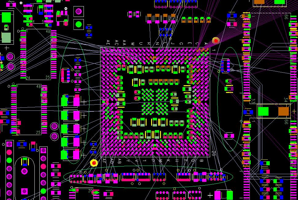
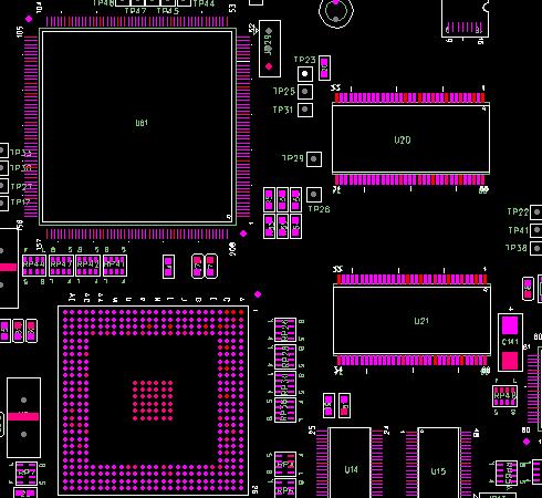
i have some queries below i am mention,still i am not complete my placement (i have some reference layout)
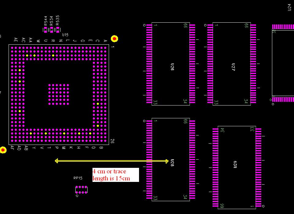
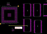
1.from MCF548x ColdFire® Microprocessor to DDR SDRAM Distance need to maintain is 4cm is it right?? or trace length should be 15cm or <6 inch right ? check the diagram
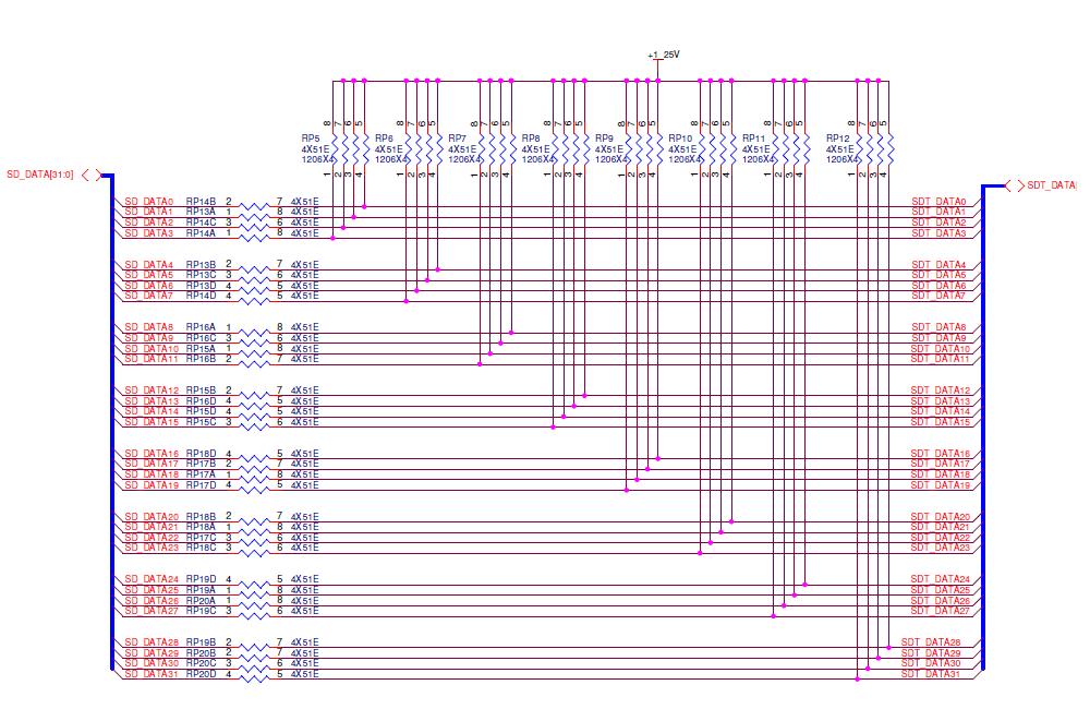
2.how to do the length match ?(i heard as per the DQS signal length i need to match the data signal right?
3.how to match the address signal??
 

My suggestion is first read about how the DDR memory works,go thru the waveforms and understand what is setup and hold time..By this you will get an idea about the relation between address,data,clk,strobes and how to do length matching...
 

As sivamani said place DDR'S one above the other so that the data signals will go as a point to point
where as for address you have to place a via inbetween the two sets of overlapped DDR'S and route address as star topology.
Regarding length matching make sure you length match the splits from the via to DDR'S equally.

Shabu.

- - - Updated - - -

Regarding length matching have a look on this it might help you.
 

Attachments

  • ddr.pdf
    819.5 KB · Views: 65

Hi everyone ,
Thanks for all to helped me.
Right now i am doing placement for Power section,i have some clarification in below point.
in my design power section (3.3V and +5V_FTR is distribute all place )2.5V for ddr power only and 1.5V processor
1.is i need to place the power section 2.5V near to DDR SDRAM or not ?? if i place power section near to ddr section (1.55A current )Thermal will affect in that area right ??
2.like that can i place 1.5V section place near to processor or not
 

Power regulators(2V5,Vref,VTT) should be closed to the Memory..by the way what is the power dissipation on 2V5 regulator?If you are using switching regulator then the drop will be less..
Regarding 1.5V place near the chip and also check the possibility of creating local power planes...
 

If you want to have rework provision in future then it is better to keep 2 to 3mm clearance to other components..
 

Hi sivamani,
Thanks for your reply.(other components means IC or decoupling capacitor) shall keep like that or marked area need to move ??


Here which is the series termination and which is parallel termination ???

- - - Updated - - -


Just maintain 2 to 3mm clearance from other components.It will be easy for assembly people ,if in case you would like to assessable and assemble it again.

Respacks which are connected to Power supply are Parallel terminations..Series means it will come in the path and should be placed near source.
 

hi sivamani,
is there any rule for test point placement because in my design has near 45 test point is there.apart from pwr and gnd can i place the test point as per net schedule enough right ??
 

It depends on you requirement how do you want to test..there is no rule as such in Test point quantity requirement.
 

Hi siva,
Thanks for your reply. how to do the routing for my board.usually first i route the power section and then i will start remaining thing. shall i proceed like that...
 

Get the stack up from fabricator
set the constraints
Power entry
Complete board fanout
Do Routing and Plane splitting plan based on number of layers availability
Route interface wise
Do length matching if required after routing
Add power planes ,make sure that there should not be any signals running over the split
make sure that all high speed signals should have good reference
then go to post routing tasks..silk & assembly etc.

If you have Signal integrity tool then u can simulate your interfaces also to check the signal quality..
 

Hi thanks for your reply,

i have signal integrity tool but i don't know how to simulate and i have another doubt also. i had seen one board file which is related DDR board only. i could not know which topology they may be used. i posted the image file please clarify my doubt

1544271300_1368155570.jpg


- - - Updated - - -

Hi thanks for your reply,

i have signal integrity tool but i don't know how to simulate and i have another doubt also. i had seen one board file which is related DDR board only. i could not know which topology they may be used. i posted the image file please clarify my doubt

1544271300_1368155570.jpg
 

check the routing how they are routed in board file. with the above placement image,it is not possible to analyze the topology..
 

Hi sir ,
can you explain this figure ??


depends on this routing will vary for example

for ddr 8 bit need to route in one layer ?? and what is lane ??
 

Status
Not open for further replies.

Part and Inventory Search

Welcome to EDABoard.com

Sponsor

Back
Top