yourdreamz
Junior Member level 1
I need to design a DC-DC buck Converter for a battery charger. Battery Capacity is 24V, 7AH. I understand the three stages of charging, viz. Bulk (Constant Current), OverCharge (Constant Voltage) and Float (Constant Voltage at a different Level). Now planning to use a microcontroller as a sensing and switching controller. So following are my queries:
Thanks in advance for all your help.
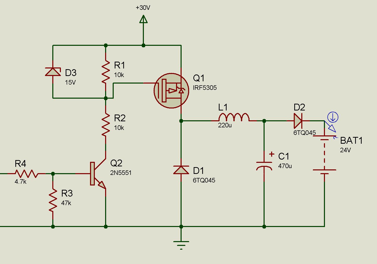
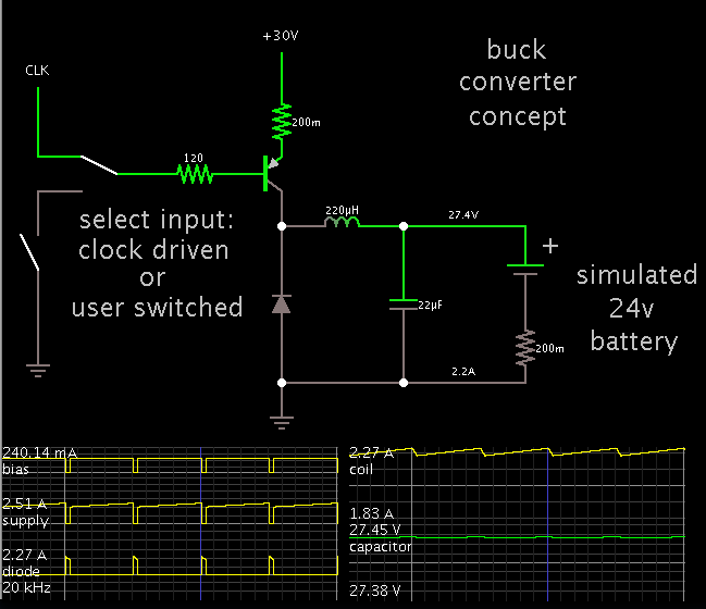
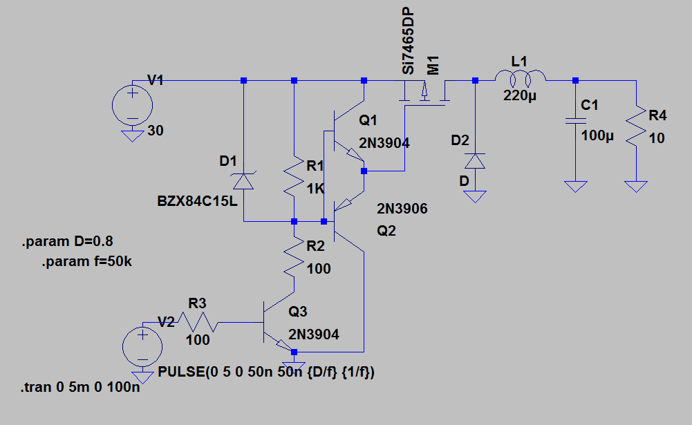
- I learnt that since the load for this Convertor (which is a battery) doesn't go to 0V, a normal bootsrtap driver with an N-Mosfet would not work. Courtesy https://www.edaboard.com/threads/239606/#post1089787. And instead of using the suggested and a little complicated techniques, could I not use a P channel MOSFET with a simple BJT gate driver instead, which I have found inexpensive and even with low Rds-on (22mOhm) like AOD4189. What's your opinion?
- Can somebody help me with a calculator or formulas for calculating the values of inductor, capacitor and diode, considering that in a Constant Current Mode the output voltage has to be varied from say 18V to 29V with current of upto 1.4 Amps in CC mode.
- And do I need to use a PID algorithm or just a normal P algorithm is good enough? (Would only P have some offset than the desired output? And is that offset okay?)
Thanks in advance for all your help.