Continue to Site

Welcome to EDAboard.com

Welcome to our site! EDAboard.com is an international Electronics Discussion Forum focused on EDA software, circuits, schematics, books, theory, papers, asic, pld, 8051, DSP, Network, RF, Analog Design, PCB, Service Manuals... and a whole lot more! To participate you need to register. Registration is free. Click here to register now.

how guard ring prevent latch up

Status
Not open for further replies.

surreyian

Member level 3
Joined
Feb 10, 2006
Messages
63
Helped
0
Reputation
0
Reaction score
0
Trophy points
1,286
Activity points
1,796
Hello,

Read a lot about guard ring prevent latch up. How exactly does guard ring prevent latch up?

There are a lot of discussion here that point out that the guard ring breaks up the SCR cause by the parasitics NPN and PNP, but I dont understand how a guard ring do that. So I dont understand how guard ring prevent latch up. Can someone explain this part in simple terms?
I attached 2 diagrams here. One is a layout without guardring and one is with guard ring. Both shows the parasitics NPN and PNP exist. I dont understand how with guard ring can prevent latch up.
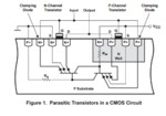
scr.PNGwith guard ring.PNG
 

You will always have the parasitic bjt's, guard rings try to minimize the chances of turning on these bjts which result in latch up. consider you get a esd current spike, and you sink that current into your nwell, via a protection diode. This large substrate current could cause enough change in the voltage in that localized nwell to create latchup. A defense for this is to decrease the resistance from the boundary of the wells to the corresponding supplies, resulting in rings bordering the wells. another method is to use a less resistive substrate , an example being an epi layer. You will also see in pad DRC files a min spacing between pfets and nfets, this is also to help reduce the chances of latchup.
 
The basic physics is very simple.

One needs to know a few basic things:

Minority carrier injection - if a p-n junction is biased in the forward direction (i.e. p-type semiconductor is positive with respect to n-type), electrons overcome the potential barrier (in the depletion region of p-n junction), and thus they are injected into p-type semiconductor. In p-type material, electrons are minority carriers, have a long life time (allowing them to travel hundreds and thousands microns, laterally). Minority carriers (electrons) either recombine, or collected (extracted) by n-wells or n+ regions (which act as potential well for electrons). Minority carriers recombine quickly (short lifetime) in heavily doped regions. Their transport is diffusion (also affected by built-in electric field from non-uniform doping), same as in bipolar transistors (in the base).

The same things happen with holes in n-type doped semiconductor (they recombine in n+ regions, and are collected by p-wells and p+ regions).

Now, referring to your drawings, if, for example, one of the n+ regions in NMOSFET is biased negatively with respect to the substrate, it will inject electrons into the substrate.
The electrons will diffuse out, until they get sucked out by n+ well.
They will lower the local potential of the n-well at the places where they are entering the n-well. This will drive them (through drift mechanism) towards n+ regions, until they are extracted from the silicon into interconnects.
Also, positive local bias of the n-well will (may) change the potential of the PMOS body - so that will act as a forward bias for p+-n-well junctions in PMOSFET.
The holes will be injected into n-well, diffuse through it, until they are extracted (or recombined) into p-substrate - then they will drift into p+ regions.
The positive biasing of the p-substrate near n+ regions will enhance electron injection - so that the positive feedback can happen, and the current may be increasing indefinitely until silicon or metal melting destroys the chip.

The guardrings help intercept the diffusion of the minority carriers - and either block their diffusion by extracting them (electrons - into n+ regions, holes - into p+ regions), or by increasing the potential barrier and decreasing their lifetime, or through some other mechanism (for example, active guard rings - that establish an electric field opposing the flow of minority carriers). Also some other techniques may be used to block the minority carrier injection or reducing the lifetime - like deep trenches, heavily doped substrates, SOI substrates, etc.

There are some good books describing latchup in detail, for example:

S. Voldman, "Latchup"
M.D.Ker at al, "Transient induced latchup..."
R.Troutman, ""CMOS latchup..."
...


Max
---------
 
So can I say with the use of guard ring, parasitics BJT will still exist.
However the guard ring/epi layer (and other latch up prevention solution) help to channel the high current to the guard ring, instead of substrate. This stops large current from building up in the parasitic BJT to substrate, hence prevent latch up?
 

yes the bjt will always be there in current cmos processes. I am not sure about SOI process though, its been a few years since ive sat down and looked at the substrate elements in those. and yes.
 

even though the parasitic bipolar transistor may still be there (with guard rings or other means to kill parasitic minority carrier effects) - it's gain can be significantly - by several orders of magnitude - suppressed.
If the gain is very low, you can say the bjt went away...
 

prestonee n timof,

It really helped me getting my head around to see how guard ring prevent latch up. thanks for detailed explanation.
 

Status
Not open for further replies.

Part and Inventory Search

Welcome to EDABoard.com

Sponsor

Back
Top