Continue to Site

Welcome to EDAboard.com

Welcome to our site! EDAboard.com is an international Electronics Discussion Forum focused on EDA software, circuits, schematics, books, theory, papers, asic, pld, 8051, DSP, Network, RF, Analog Design, PCB, Service Manuals... and a whole lot more! To participate you need to register. Registration is free. Click here to register now.

operational amplifier driving a resistive load

Status
Not open for further replies.

Junus2012

Advanced Member level 5
Joined
Jan 9, 2012
Messages
1,552
Helped
47
Reputation
98
Reaction score
53
Trophy points
1,328
Location
Italy
Activity points
15,235
Hello once again and again

as normal, I always has many questions since I started my analog project :-D.

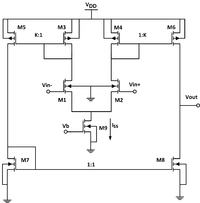
the question is, How we assume in the operational amplifier driving a resistive load that all the biasing current is passing in this load while the amplifier is working with a negative feedback. from the principle of the negative feedback, the difference voltage at the operational amplifier is forced to be zero, thus the op-amp is under the small signal condition and the output current to the load should be zero (of we assume no transient time at the output).

Hope it is clear for you

Thank you
 

the difference voltage at the operational amplifier is forced to be zero, thus the op-amp is under the small signal condition and the output current to the load should be zero

Why do you think so?
 

I mean the difference at the op-amp inputs are forced by the negative feedback to be zero (with very high op-amp gain)

OK- nearly zero.
Is that the reason you think the output current also would tend to be zero?
 

yes, the output current to the load is in this case is zero (the sourcing current = sinking current, hence Iload=0),


OK- nearly zero.
Is that the reason you think the output current also would tend to be zero?
 

yes, the output current to the load is in this case is zero (the sourcing current = sinking current, hence Iload=0),

Junus, what means "in this case"?

The other way round: In which case - do you think - it is not zero?
 

all the biasing current is passing in this load
What do you mean with "all the biasing current"? It's far from a clear question. How about a schematic with currents marked?


What do you mean with "all the biasing current"? It's far from a clear question. How about a schematic with currents marked?

- - - Updated - - -

with the current mirror ota, assume VID = 0, I6=I8, therefore I out =0.

Again here is my question, we usually run the op-amp with a negative feedback. Hence we usually have the VID=0 and Iout =0. so how the connected load resistor will have the current???
 

You are confusing theory of ideal OP with real circuit operation. VID = 0 applies to an ideal OP with infinite gain only. A real OP with finite gain will show a small Vid according to the output voltage respectively current.

Secondly your circuit is an OTA, no voltage mode OP. It has well defined transconductance gm (in small signal operation) respectively a tanh() transfer characteristic for larger output currents. Most OTA specific applications are working based on a defined gm value, e.g. gm-C filters, and not assuming infinite gm.

While assuming infinite gain may be suitable for simplified OP calculations, it's generally wrong for OTA circuits with load.
 
Again here is my question, we usually run the op-amp with a negative feedback. Hence we usually have the VID=0 and Iout =0. so how the connected load resistor will have the current???

Junus - independent on FvM`s question, WHY do you think that Iout=0 results from VID=0 ?
Even from the mathematical point of view a zero input voltage multiplied with an infinite gain can result in a finite output voltage, which is able to drive a load current.
 
Status
Not open for further replies.

Part and Inventory Search

Welcome to EDABoard.com

Sponsor

Back
Top