axismundi
Newbie level 3
Hi all,
A few days ago I have created a custom pad shape in Altium to be used at the end of a FPC (ZIF connector). All went apparently well and I was able to draw the desired circuit, however when exporting the circuit to Gerber and using gerbv to view the file I noted something strange: within each pad there is a thin "island" which is not covered by cooper.
Attached a print screen from gerbv vs. the original as shown by Altium:
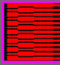
 Gerber file opened with Grbv
 original design in Altium
I have no clue why this is the case, hence looking for help.
Some more info:
- I have created the pads by drawing first the outlines and then converting to regions; I'm pretty sure that this is where the trick lies as prior to the current shape I had a slightly different version, drawn using different tolerances / dimensions (mm vs mil in latter) and the Gerber export had been even worse (some pads did not show up at all)
- The pads are tiny (e.g. the thinnest portion and the spacing measure just 4 mils)
- I have prepared the Gerber files using a tried and tested method (true, never with circuits including custom pad shapes and never with traces smaller than 8 mil)
- I tried some other Gerber viewers and the result is the same.
Thanks in advance.
A few days ago I have created a custom pad shape in Altium to be used at the end of a FPC (ZIF connector). All went apparently well and I was able to draw the desired circuit, however when exporting the circuit to Gerber and using gerbv to view the file I noted something strange: within each pad there is a thin "island" which is not covered by cooper.
Attached a print screen from gerbv vs. the original as shown by Altium:
 Gerber file opened with Grbv
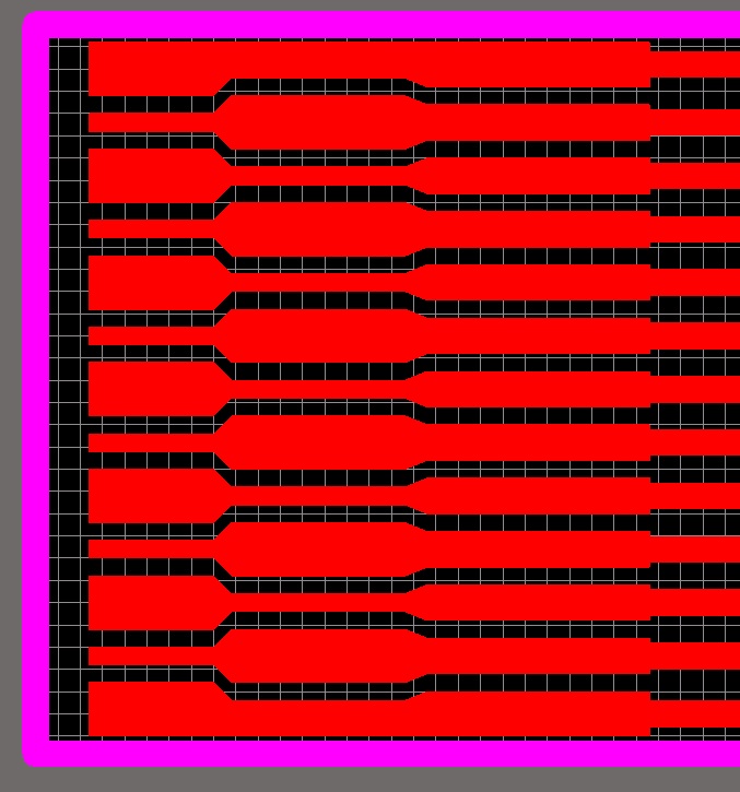 original design in Altium
I have no clue why this is the case, hence looking for help.
Some more info:
- I have created the pads by drawing first the outlines and then converting to regions; I'm pretty sure that this is where the trick lies as prior to the current shape I had a slightly different version, drawn using different tolerances / dimensions (mm vs mil in latter) and the Gerber export had been even worse (some pads did not show up at all)
- The pads are tiny (e.g. the thinnest portion and the spacing measure just 4 mils)
- I have prepared the Gerber files using a tried and tested method (true, never with circuits including custom pad shapes and never with traces smaller than 8 mil)
- I tried some other Gerber viewers and the result is the same.
Thanks in advance.