newbie_rf
Junior Member level 3
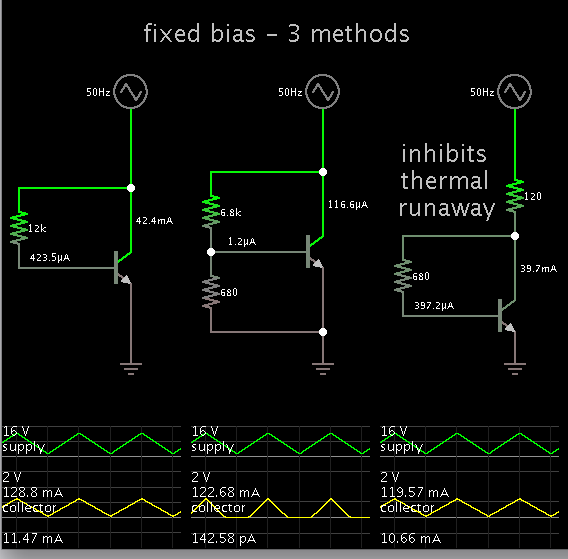
I am trying to manually check how adding a base resistor can reduce Ic sensitivty regarding to base terminal bias voltage Vb.
Since it is a simple common emitter BJT transistor (emitter directly to ground, collector directly to Vcc),
So Ic=K*exp(Vbe/Vt)
where Vbe=Vb-(Ic/beta)*Rb
Therefore, Ic=K*exp{[Vb-(Ic/beta)*Rb]/Vt}.
Now Ic (which is Y) vs. Vb (which is X) is a transcendetal equation that cannot be easily solved.
How do I evaluate the Ic sensitivity with regard to Vb, without resorting to a simulation tool?
Another question is how much Rb is really needed to stabilize Ic?
Any comments or insight is much appreciated.