adeel abid
Junior Member level 3
Dear All,
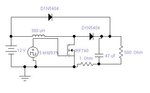
i have designed a boost converter. It is based on IRF740. Driving gate signal is generated by microcontroller which is then pulled up with !k resistor to 12V. So Vgs is either 12V or 0V with ton=190us and min. toff=10us giving about 93.3% duty cycle.The gate driving signal is not continuous but actually based upon monostable multivibrator that is only trigerred if load voltage is less than desired value & simultanoeusly indcutor current is reduced to zero (this is sensed by sensing voltage across 1ohm resistor).
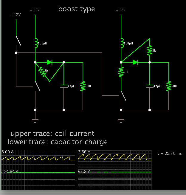
Problem i am facing is that when MOSFET is on for 190us as per ideal calculation id should be ramp with ID(max)=8A. During this phase only the battery, inductor and IRF740 is in the circuit. But practically after implementation i am getting ID(max)=3.5 to 4A (measured by sensing peak voltage acorss 1 ohm resistor).
There is not so much heating of IRF740 to increase RDs(on) to limit the drain current to this value because i have tested it with no load i.e. without 500 ohm resistance (and hence multivibrator pulse repetition period is quite large to allow cooling between generation of pulses). This is limiting the input power of boost converter and hence the output power delivered to the load.
please provide reason for this behaviour.
Thanks in advance.
i have designed a boost converter. It is based on IRF740. Driving gate signal is generated by microcontroller which is then pulled up with !k resistor to 12V. So Vgs is either 12V or 0V with ton=190us and min. toff=10us giving about 93.3% duty cycle.The gate driving signal is not continuous but actually based upon monostable multivibrator that is only trigerred if load voltage is less than desired value & simultanoeusly indcutor current is reduced to zero (this is sensed by sensing voltage across 1ohm resistor).
Problem i am facing is that when MOSFET is on for 190us as per ideal calculation id should be ramp with ID(max)=8A. During this phase only the battery, inductor and IRF740 is in the circuit. But practically after implementation i am getting ID(max)=3.5 to 4A (measured by sensing peak voltage acorss 1 ohm resistor).
There is not so much heating of IRF740 to increase RDs(on) to limit the drain current to this value because i have tested it with no load i.e. without 500 ohm resistance (and hence multivibrator pulse repetition period is quite large to allow cooling between generation of pulses). This is limiting the input power of boost converter and hence the output power delivered to the load.
please provide reason for this behaviour.
Thanks in advance.