Vermes
Advanced Member level 4
Presented here project consists of home made alternatives of M5207L01 and double operational amplifiers in SIL housings. SMT was used to reduce the size of device. This design is perfect for all people who connected the internal supply of BOSS incorrectly or for those who want to build a clone. BOSS supply has a ground inside and plus 9V outside, so when you connect it reversely, you can damage the device – so presented here project is a solution for that problem.
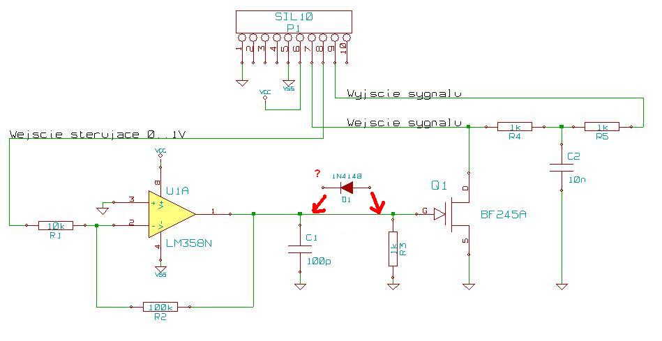
M5207L01 is a double, voltage controlled, linear silencer. Control voltage is in the range of 0...1V (0V – there is no signal and 1V – the same is at the output and at the input). NS-2 is a noise gate, which is triggered at a certain level set by THRESHOLD potentiometer, for a certain period of time which can be set by another potentiometer. That system is responsible for smooth cutting off the signal. Voltage then drops from 1V to 0V and cutts off the signal from a guitar.
Transistor BF245A was used in that project, because the supply voltage is about 4,5V (it is artificial ground, because it is powered from 9V battery or power supply). The transistor should short the signal to the ground, so the right signal does not go through it. In that way the noise is smaller. In addition, there are resistors in 10x filter at the input and the capacitance is 10x decreased. Output buffer was removed, because it had made the signal too strong. All the components could be experimentally selected, because it is difficult to calculate anything.
There is an amplifier at the control input, which inverts and strengthens the control signal. JFET operates in the following way: if you connect the gate to the ground, current flow between the source and drain, when the voltage is negative, it starts clogging. Operational amplifier LM358 (the same as in double alternatives OPAM in SIL) was used to do that.
NOTE! There is a diode D1 marked on the schematic below, there is a jumper in that place, because the voltage drop on it causes the transistor did not clog totally. It is adviced to perform tests with and without the jumper.
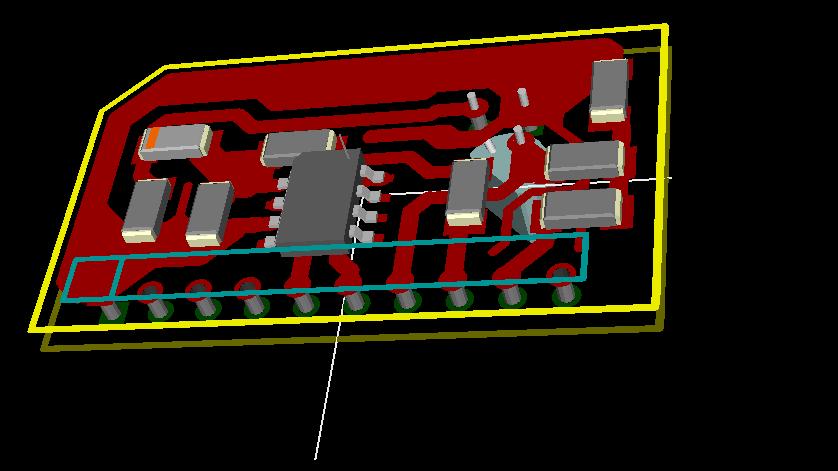
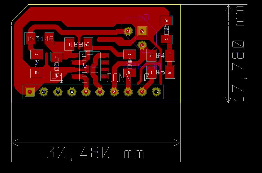
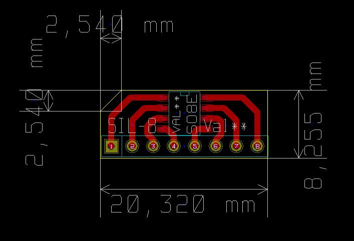
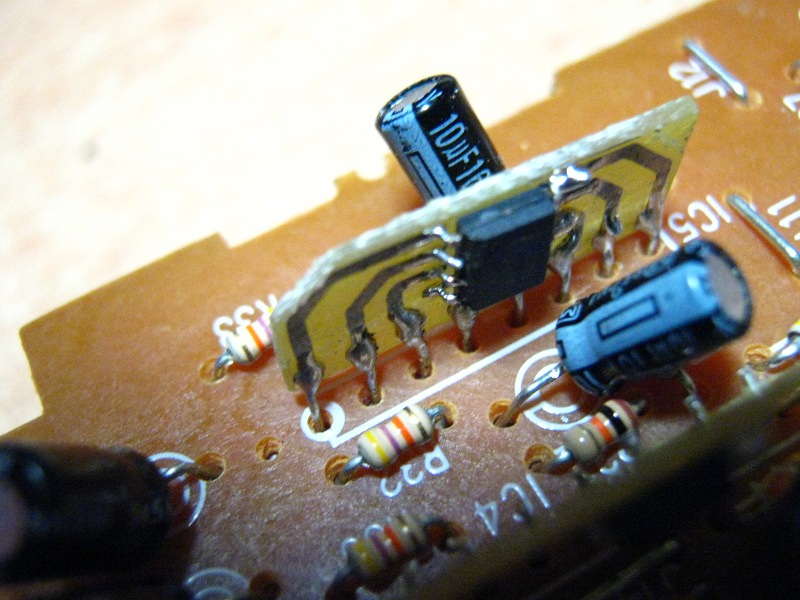
Operational amplifiers consists of two ordinary amplifiers in SIL housings. They can be made of LM358 SMD on small boards.
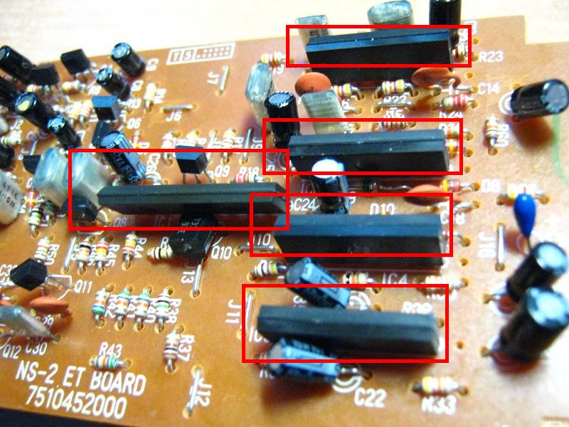
Diode D1, which is connected in parallel to the supply, should be exchanged, such as capacitor C1, because it is electrolyte which should not be with reverse supply. C25 10uF should be changed to 1uF and R18 2,2k to 22k.
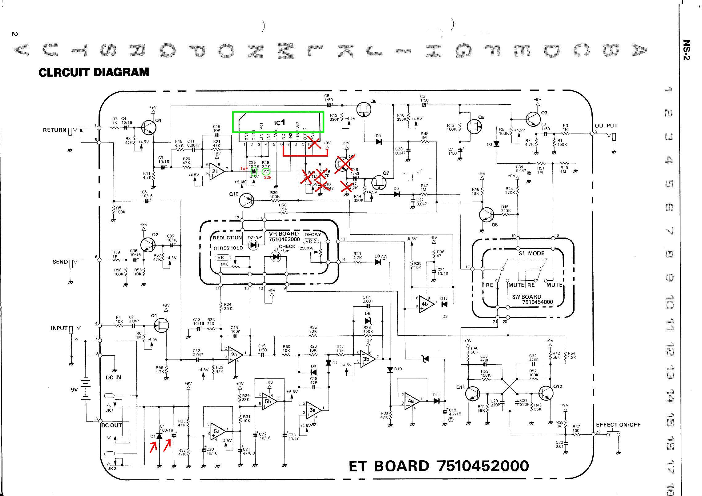
R15, R16, R17, C10, Q9, jumper of pin 10 to pin 6 should be deleted.
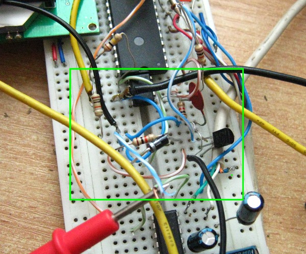
Link to original thread (useful attachment) - Zamienniki DIY układu M5207L01 i innych do bramki BOSS NS-2