Continue to Site

Welcome to EDAboard.com

Welcome to our site! EDAboard.com is an international Electronics Discussion Forum focused on EDA software, circuits, schematics, books, theory, papers, asic, pld, 8051, DSP, Network, RF, Analog Design, PCB, Service Manuals... and a whole lot more! To participate you need to register. Registration is free. Click here to register now.

ASIC design flow QUESTION

Status
Not open for further replies.

achundur

Junior Member level 1
Joined
Feb 24, 2012
Messages
19
Helped
0
Reputation
0
Reaction score
0
Trophy points
1,281
Activity points
1,448
Hi all :

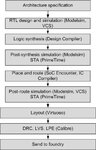
I synthesized a VHDL design and the post-layout (without SDF annotation) simuation is working. But when I tried to do back-annotated simulation of the design using Nc-sim by reading SDF file (generated by Design compiler) , I observed that clock signal is sampling the glitch instead of capturing the data. This occured because clock skew and the reason for clock-skew is clock-gating logic in clock-path.

How should I proceed now? When does the prime-time comes into picture? What is next step after synthesizing a desin in ASIC flow?

Thanks
 

After synthesis DFT logic is inserted into the synthesized netlist and this netlist is given to physical design team. Physical design does floorplanning, place, clock tree synthesis and routing. Prime time is timing analysis tool used to check whether we meeting timing constraints or not .
https://en.wikipedia.org/wiki/Physical_design_(electronics)
 
Simple design flow from rtl to foundry:
 

Attachments

  • asic design flow.jpg
    asic design flow.jpg
    34 KB · Views: 130
Simple design flow from rtl to foundry:

This flow doesn't include dft process, like mbist, scan chain, atpg & bsd.
If dft process above is included, the flow will be a bit longer.
 

This flow doesn't include dft process, like mbist, scan chain, atpg & bsd.
If dft process above is included, the flow will be a bit longer.

That's correct as I'm not familiar with DFT flow. Here is the DFT flow using Synopsys tools:

1. HDL design considering Testing
==> you can check Synopsys RTL TESTDRC check with DFT compiler
==> Memory : Memory BIST logic insertion

2. Synthesis considering Scan : DC Compiler
==> compile -scan ( pre_compiled with scan)
==> this command make F/F ==> scan F/F
==> check_test or check_dft : check DFT Violation Rule

3. SCAN insertion & make chain : Synopsys DFT compiler
==> insert_scan or insert DFT
==> this command make scan chain
of course , we have to cofigure scan chain

4. BSD(JTAG) insertion with Synopsys BSD compiler
==> insert_bsd
==> you can insert JTAG before synthesis.
==> Make BSD vector with BSD compiler

5. ATPG with Synopsys Tetramax

==> make ATPG vector with Tetramax
==> get fault exact coverage
==> if you want , you can fault_simulation.

6. Simulaiton ( ATPG , MBIST , JTAG)

==> simulate all vector with your simulator ( ncsim or vcs or others)

Source: https://www.edaboard.com/threads/8823/#post35637

I think those flow must be done before P&R step.

Thank you.
 
Status
Not open for further replies.

Part and Inventory Search

Welcome to EDABoard.com

Sponsor

Back
Top