NVergunst
Member level 1
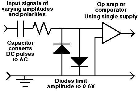
I have an input signal which can be any of the following (maybe others in the future too):
a true +/- sine wave of +400mV to -400mV
a true +/- sine wave of +6V to -6V
a square wave signal between 0V and anything between 3V and 15V
There are little variations in those as well (like rectified positive humps instead of a true square wave for instance) but those are the main input signals.
I then need to convert this signal to a 0V to VDD (3.3v or 5v) signal with a square wave. Duty cycle is not very important, the frequency is what is important. Phase shifting is OK too. Basically counting edges.
So I am entertaining ideas on how to make a generic input that can take these small signals below a diode drop and these big signals above VDD and magically make them digital lol.
I was thinking something like a zener diode for the higher voltages could be sent into a comparator with the other side of the comparator at VDD and ground. Then for the small signals an amplifier with some gain then through another comparator. Using the zener turn on I could maybe switch a FET to disconnect the small signal input to the comparator.
I wondering if there is an already general solution to these types of problems so I am not reinventing the wheel. All suggestions are welcome, Thanks.