Continue to Site

Welcome to EDAboard.com

Welcome to our site! EDAboard.com is an international Electronics Discussion Forum focused on EDA software, circuits, schematics, books, theory, papers, asic, pld, 8051, DSP, Network, RF, Analog Design, PCB, Service Manuals... and a whole lot more! To participate you need to register. Registration is free. Click here to register now.

How does IR2110's HIGH-SIDE Internal Circuity work ?

Status
Not open for further replies.

TripACT

Member level 3
Joined
Apr 2, 2012
Messages
56
Helped
3
Reputation
6
Reaction score
3
Trophy points
1,288
Activity points
1,739
How does IR2110's HIGH-SIDE Internal Circuit work ?

I think i understand how this driver work with only high-side configuration for buck converter.

i'm trying to understand how the high-side section works internally.

IR2110 Internals.PNG

haven't found anything on the web so far.

experts? :roll:

Gary
 

Dear Gray
Hi
Are you referring to the boot strap section ? is your problem with understanding how it can drive h side mosfet ? or you are referring tot he internal sections ?
If internal section is your mean :
At first it will have two mosfet as voltage multiplier and then an under voltage lockout . this section is prepared to control dissipations due to the low gate drive supply . if your gate supply ( GS ) be lower than 15 volts , your mosfet will be at linear region that means dissipative region . this section will shut down your IC , if your supply isn't as much as enough .
Best Wishes
Goldsmith

Hi my friend,

i did looked for understanding the internal secions.
thank you for your explanation.

Are you referring to the boot strap section ? YES
Is your problem with understanding how it can drive h side mosfet ? YES

Of course these questions i would also ask...

I do want to understand how this bootstrap section works. For my understanding, here it consists of a capacitor and diode ? yes ?
this bootstrap thing always made me confused. sure i can also tell that this source connection to Vs HIGH SIDE OFFSET voltage also adds to the confusion.

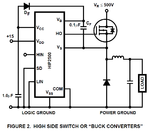
will be happy to understand how it works in this circuit:

highside switch.PNG


Thank you :)

Gary
 

Hi again My friend
At first the circuit that you attached has a big problem ! this mosfet can't be turn on ! never ! because boot strap capacitor won't have any path to be full of charge . hence you should use another mosfet which has an internally anti parallel diode instead of the diode in out put section .
Anywhere , Wait for some minutes , please , i'll write some paper for you , and i'll attach them for you , . just some minutes .
Best Wishes
Goldsmith
 

i'm sorry to disturb you while you make some papers,

but actually i simulated it in pspice and it works. are you sure with your claims ?
the topology i attached earlier was taken from a datasheet.

here's the pspice schematic:

my_schematic.PNG

VDD Supply voltage is 12vdc.

Gary
 
Last edited:

Well i came back , see below , please :
View attachment IMG_0969.pdf
View attachment IMG_0970.pdf
You can also , remove negative supply and use ground instead of it for your aim . and i saw it's datasheet and then i told this to you . if you read things that i wrote i think you'll understand my meaning . and nother thing is , that simulation can't show you all things !
BTW : sorry if my hand writing is bad !
Best Wishes
Goldsmith
 

Dear goldsmith,

Thank you very much for your dedication!

Here's a question: won't the hexfet IRF540N should with be sufficient applying according to the datasheet schematics without the need of another moset? I just need it for buck converter and not for implanting any kind of bridges, using only HIN input, and high-side outputs...

Update: btw, the buck's vin should be anything between 1v and 41v approx.
 
Last edited:

Cubano,

Thank you for those links.

The application note an-978 I did try to read. It was mister-rf who supplied me with that link on another thread, but the boot strap explanation was too complicated that I couldn't get it's general purpose.

The other application note you recommend seems to have planty explanations in depth. Hope that I could understand its usage.

I will try to look into it.
 

Hi again
I'm glad because i could help you .
But , it is a usual term to use a mosfet instead of diode or a mosfet in parallel with diode . however there are some float drivers that designed just for H side . but majority of drivers need two mosfet , too . such as IR21XX (2113 /2110 /2130 .... )
Good luck
Goldsmith

- - - Updated - - -

By the way , i'm glad too , because you could read my bad hand writing !
 

So I didn't understand...is the IRF540N sufficient without the need for another MOSFET? It had an internally schotkey diode connected between the source and drain. The driver I'm using is IR2110
 

oh sorry i forgot to answer this question !
At first , what do you mean by : it has internally diode ? pf course it has but what is the benefit of this diode in driving process ? nothing !
Can you attach it's datasheet , please ? IS2110 ?
 

I'm sorry, it was a typo... I meant IR2110 Driver. Already corrected it in my reply.


Gary
 

Gary , of course you'll need low side mosfet too , ( for this driver ) but don't forget to create enough dead time . if you create enough dead time , the low side mosfet can be a low power mosfet and then you can use a high power diode in parallel because the low side mosfet in your aim , is just to supply bootstrap capacitor ( creating a path up to ground )
Good luck
Goldsmith
 
Okay, i understand now, thank you very much !

i tried to take a look on the application notes regarding the bootstrap topology and still can't understand why the hell do we need it at all ?
what happens if we dont apply bootstrap configuration to high-side drive circuit ?

Gary
 

Hi again dear Gary
Ha ha ! i see ! i know exactly what is in your mind ! listen carefully ! we will have a PWM or SPWM . which has a ground ( reference point ) . and we will have a high power power supply . . and as you probably know we have to put +15 volts across the GS junction of each mosfet to turn it on . you understand ?
So for low side , we won't have any problem because we can connect or signal ground ( ground of PWM section ! ) to the source of low side . but we can't connect it to the source of H side too . because if we do it , in fact , we should see a big explosion ! because the DS of l side short circuited if we do it !
So we should create a float supply to drive h side .
Clear ? if you don't understand it , tell me , please i can simplify it for you .
Good luck
Goldsmith
 

Consider a high side NMOS switch. To drive the output to postive supply (fully on), what's the required gate voltage referred to positive supply? What are your options to generate the gate-drive voltage?
 

yes i read that the gate voltage must be 10-15 volts higher than the source voltage. so are you saying the that the bootstrap capacitor solves it by charging itself to VDD-Vf(Bootstrap Diode)
so the gate's peak voltage would be VIN(Buck)+VDD-Vf(Bootstrap Diode) like said on other topic ?
 

the gate voltage should be around +HV+15 ! the GS voltage is +15 volts !

- - - Updated - - -

e.g your VDC is around 500 volts ! the voltage from gate up to ground , will be 515 volts . but GS voltage will be 15 volts !
 

2 questions:

1. if i tied together my PWM outputs via diodes to have the whole duty cycle range (using SG3525A), instead two outputs with 180 degree phase difference.
i understand that now two mosfets need to be used on the output to fully charge the bootstrap capacitor (VCC to groun) i see LIN has to be used as well.
BUT - in my schematic i used only HIN connectivity. LIN is grounded. what do i connect to LIN in my driver?

2. is using two mosfets with an external diode equal to using two hexfets with their internal diodes ? so no need for external diode ?


Gary
 

Status
Not open for further replies.

Similar threads

Part and Inventory Search

Welcome to EDABoard.com

Sponsor

Back
Top