Continue to Site

Welcome to EDAboard.com

Welcome to our site! EDAboard.com is an international Electronics Discussion Forum focused on EDA software, circuits, schematics, books, theory, papers, asic, pld, 8051, DSP, Network, RF, Analog Design, PCB, Service Manuals... and a whole lot more! To participate you need to register. Registration is free. Click here to register now.

Impedance relation between 2 Bjts

Status
Not open for further replies.

samy555

Full Member level 4
Joined
May 11, 2010
Messages
207
Helped
0
Reputation
0
Reaction score
0
Trophy points
1,296
Location
Palestine
Activity points
2,963
Hi
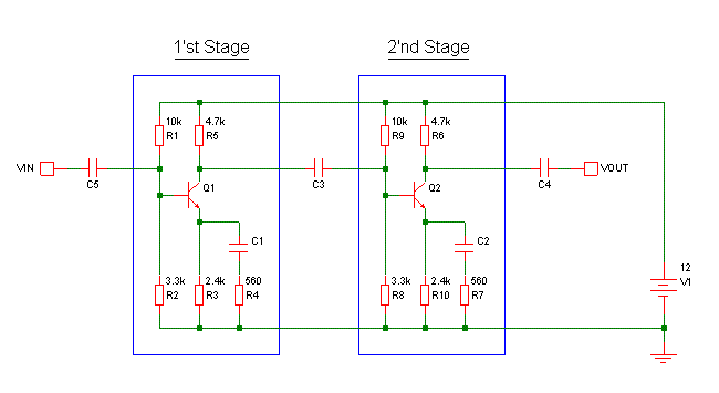
If there are two BJT small signal amplifiers (common Emitter) cascade connected using a suitable decoupling cap
The first preamp has an o/p imeadance Zo, and the second has an i/p impedance Zin
Now we have Zo and Zin and a cap betwwen them
My question is: Is the connection series or parallel? That, is the o/p voltage divided or the o/p current?
 

Dear samy
Hi
What do you mean by o/p and i/p ? . and what you mean by "Is the connection series or parallel" ? if you tell me a bit more explanations , perhaps i can help you .
Best Wishes
Goldsmith
 

I think i/p and o/p mean input and output, and that he is talking about a circuit like the one below.

Each gain stage, if used on it's own, would have Zin = 2.5K, Zout = 4.7K, and signal voltage gain = 10.

When they are connected together as shown, Zin of the 2'nd stage is in parallel with Zout of the first stage, so the voltage gain of the first stage is reduced by a factor of 3 (approximately).


Dear godfreyl
Hi
In your example , you mentioned that zin=2.5k . how you calculated it ? i don't think that it is correct . because you simply used this equation :R1llR2 . and why you used a resistor in series with bypass capacitor ? to control the gain ?
(Zin=R1llR2llbeta(re+RE))
Best Regards
Goldsmith
 

Zin=R1 ll R2 ll beta*(re+RE)

You are totally right. He just neglected beta*(re+RE) being relatively high (about 100K typically, if not higher).
 

Hi Goldsmith

Yes, the resistor in series with the bypass capacitor is to set the voltage gain to 10, which seems like a useful value. Without the bypass capacitor and resistor, the gain will only be about 2. If we have the bypass capacitor without the series resistor, the gain will be very high, but the distortion will also be high and the input impedance will be low.

To calculate the input impedance, I ignored the "beta(re+RE)" term as it will be very high and make very little difference. With a transistor such as BC547C, beta(re+RE) will be between about 100K to 200K.

Regards, Godfrey
 

Dear godfreyl
Hi
Yes , you're quite right . with a good approximation , we can say 2.5 k .
Best Regards
Goldsmith
 

Dear SunnySkyguy
Hi
the link that you attached has many helpful things ! i will suggest it to many of my friends who love these things .
Thanks
Goldsmith
 

I think i/p and o/p mean input and output, and that he is talking about a circuit like the one below.

Each gain stage, if used on it's own, would have Zin = 2.5K, Zout = 4.7K, and signal voltage gain = 10.

When they are connected together as shown, Zin of the 2'nd stage is in parallel with Zout of the first stage, so the voltage gain of the first stage is reduced by a factor of 3 (approximately).


Yes thats what I mean.
my question was: If Zin of the 2'nd stage = say 10K, and Zout of the first stage = 10 Kohm< is these two impedances connected parallel or series?
Your answer was that's in parallel, but from "the art og electonics" book, page 66
jb13363330631.jpg

Is meant by saying that the connection is in series and I think that he's true
 

Hi Samy,

Both views are true :)

They are parallel, if we look to know the load at the Q1 collector for example.
Proof: If we short circuit R8 (hence Zin=0), the AC voltage at Q1 collectror would be zero.

They are also in series with the bypass capacitor C3 (for calculating its value for example).
C3 blocks the DC voltage and the AC low frequencies (as in a high pass filter).
Proof: If we remove Zin and replace it with 10M resistor (almost open circuit), the cutoff frequency would be very low even if C3 has a very low capacitance.
Fc = 1 / [ 2 * PI * C3 * (10000000+4700) ]
Also in this case, the load at Q1 collector is very close to R5 (4K7)... 4K7 // 10M

Kerim
 
Last edited:

Both views are true :)
Yes, good thinking.
The output of the first stage can be thought of as either a voltage source in series with the output impedance, or a current source in parallel with the output impedance.
 
  • Like
Reactions: KerimF

    KerimF

    Points: 2
    Helpful Answer Positive Rating
Yes, good thinking.
The output of the first stage can be thought of as either a voltage source in series with the output impedance, or a current source in parallel with the output impedance.
But when should be considered as a voltage source in series with the output impedance, or a current source in parallel with the output impedance?
thanks alot

---------- Post added at 15:21 ---------- Previous post was at 15:12 ----------

Yes, good thinking.
The output of the first stage can be thought of as either a voltage source in series with the output impedance, or a current source in parallel with the output impedance.
But when should be considered as a voltage source in series with the output impedance, or a current source in parallel with the output impedance?
thanks alot
 

Dear samy
Hi
As you probably know , each transistor is a current source ( it has a voltage source internally but it's effect isn't high and we will neglect from it's effect ) . so as you probably learned at circuit analysis , if we have a current source with a parallel resistor , we can change it's model to the voltage source and a series resistor .
ok ?
Best Wishes
Goldsmith
 

Yes, good thinking.
The output of the first stage can be thought of as either a voltage source in series with the output impedance, or a current source in parallel with the output impedance.
But when should be considered as a voltage source in series with the output impedance, or a current source in parallel with the output impedance?
thanks alot
 

It depends on your abilities ! we will use the theorems of circuit analyzing to simplify the circuit ! for example we can solve each linear circuit with super position law and we can solve it with potential of node way . it depends on you . but about transistor , i didn't change that current source to the voltage source at transistor , ( never )
Best Luck
Goldsmith
 

Hi Samy... I am just curious to know what you couldn't get from my post #11.
 

Hi Samy... I am just curious to know what you couldn't get from my post #11.

Im sorry,
At first I did not understand you
But now I got you completely
In order to assure I am now asking you personally:
Suppose i have a signal source of 10mVp (ignore the internal impedance of that source)
this 10mVp signal is applied to the input of a transistor preamplifier has voltage gain Av=10 and output impedance Zout = 5 Kohm
At the collector of this transistor preamplifier, I connect a load resistor of 5 Kohm through a suitable coupling cap
Is the Voltage across the Load = 0.5 *10* 10 = 50 mVp? that is voltage divider???
 

Samy another way to consider your original question, is that since your design is not an ideal voltage source for each stage, you must consider they are serial stages but with parallel loading effects.

That is why I suggested making each stage at least 10x higher Rin vs Rout..., so that I can optimize the gain and consider each stage as a serial stage with minimal parallel loading affects.

Your choice of Base bias resistors makes for very stable bias point at huge expense to AC gain.

Consider let AC Voltage gain = 10
and Impedance gain Rin/Rout =10
Rin2~{R9//R8} // hFE*{R10 // (R7+1/ωC2)}
where // means parallel equiv cct. and hFE =β of Q2 which is usually>>100

Yes
I get it,,, thanks SunnySkyguy
 

Status
Not open for further replies.

Similar threads

Part and Inventory Search

Welcome to EDABoard.com

Sponsor

Back
Top