Continue to Site

Welcome to EDAboard.com

Welcome to our site! EDAboard.com is an international Electronics Discussion Forum focused on EDA software, circuits, schematics, books, theory, papers, asic, pld, 8051, DSP, Network, RF, Analog Design, PCB, Service Manuals... and a whole lot more! To participate you need to register. Registration is free. Click here to register now.

[SOLVED] trace thickness in ADS

Status
Not open for further replies.

grit_fire

Member level 5
Joined
Mar 13, 2011
Messages
82
Helped
1
Reputation
2
Reaction score
1
Trophy points
1,288
Location
USA
Activity points
1,966
Hi, all,

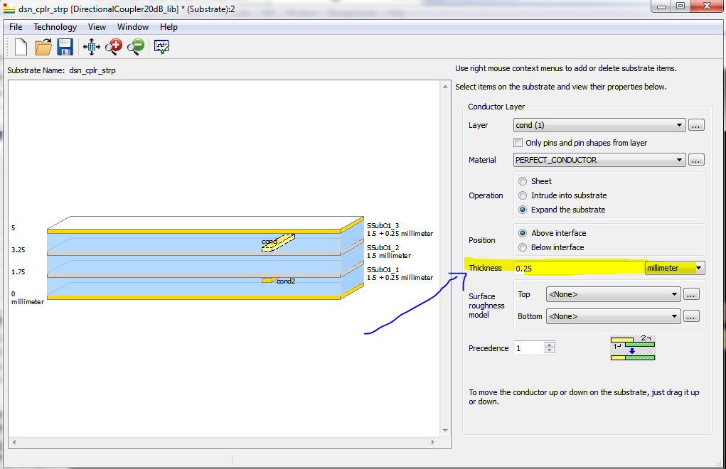
I cannot find the place to define the thickness of a trace in ADS 2011.5.

In older version, I can do that easily. But now, it seems this is impossible. Does anyone know how to set the thickness of a trace? I believe that is an important parameters for antennas or transmission lines.\

Thanks a lot!
 

Thickness in circuit model or in the EM substrate definition?
 

Thickness in circuit model or in the EM substrate definition?

I was referring to the trace thickness in the layout window. Thank you

---------- Post added at 00:43 ---------- Previous post was at 00:42 ----------

Thickness in circuit model or in the EM substrate definition?

And that shd be em simulation, but not substrate thickness, which i can define
 

I was referring to the trace thickness in the layout window.

Why do you want to set a trace thickness in layout? Does not make sense to me, because the layout is 2D.

And that shd be em simulation, but not substrate thickness, which i can define

I don't understand your problem. You can set the thickness, see screenshot


Why do you want to set a trace thickness in layout? Does not make sense to me, because the layout is 2D.


I don't understand your problem. You can set the thickness, see screenshot


Thank u!thats wat i am talking about.

Btw it is 2.5D instead if 3D actually. I care because the skin depth factor. Need to consiser the thickness.
 

I care because the skin depth factor. Need to consiser the thickness.

Sure, that is why I asked about circuit (model based) simulation or EM simulation.
For model based simulation, you specify the thickness in the substrate block (MSUB).
For EM based simulation, you specify the thickness is the substrate definition.
 

Status
Not open for further replies.

Part and Inventory Search

Welcome to EDABoard.com

Sponsor

Back
Top