Continue to Site

Welcome to EDAboard.com

Welcome to our site! EDAboard.com is an international Electronics Discussion Forum focused on EDA software, circuits, schematics, books, theory, papers, asic, pld, 8051, DSP, Network, RF, Analog Design, PCB, Service Manuals... and a whole lot more! To participate you need to register. Registration is free. Click here to register now.

Capacitive DAC array in SAR A/D

Status
Not open for further replies.

cmos_ajay

Full Member level 2
Joined
Jan 30, 2007
Messages
126
Helped
0
Reputation
0
Reaction score
0
Trophy points
1,296
Activity points
2,247
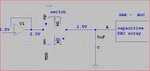
Hello, I have a unity gain buffer connected to a switch and a big capacitor of 5uF. It supplies a 2.5V to a capacitive DAC array in a SAR A/D converter. When the most significant capacitor (MSB) in the DAC array is switched at a certain frequency, the voltage at node A keeps falling by a few uV every clock cycle. I would expect the voltage to remain stable at around 2.5V always.

But if I remove the switch and replace it with a short, the voltage at node A remains stable for all clock cycles .
* I believe the switch resistance is causing the capacitor C to discharge by a few uV with every clock cycle .

Is there any solution for this since I need to use a switch in my design ??
Please see attached picture.
 

Attachments

  • SAR - ADC.JPG
    SAR - ADC.JPG
    85.5 KB · Views: 93

I do not know what models you use but there are always parasitic resistances that are connected to supposedly floating nodes. So it is expected that when you open circuit the capacitor with the transmission gate, it will discharge in time. If you are asking for an error of uV per cycle when the transmission gate is always short circuited, it might be a settling issue caused by driving the capacitor via a resistance. Could you please run a longer simulation and see if this holds true?

The thing is when you reduce the resistance with larger transmission gates, the charge injection increases and you lose accuracy of uV's already. An optimization is necessary if this causes an error more than 1 LSB.

Also you are going to open and close that switch. Every time you do that you are going to charge a 5uF capacitor ,which is quite large to realize reliably in IC's by the way, this will increase your power consumption. I do not know speed specifications for your design but consider hybrid DAC's as another solution.

I hope this helps.
 

Hello, I checked the frequency response of the above configuration. It has very low bandwidth also . It seems stable, but I believe due to the large load capacitor, the pole at the output side has moved to a very low frequency. Should I use a single stage amplifier instead of the 2 stage for the buffer. It is difficult to compensate 2 stage opamp with such a high load capacitor in series with switch resistance (small). I will appreciate your reply.
 

Try OTA then. But be advised you are going to lose some gain also. So the accuracy of your Vref voltage will be lower than before. It should be within 1 LSB. But again 5uF is a very large capacitance.
 

Hello Kemiyun, I agree a OTA will be better with less accuracy. Its dominant pole will be due to o/p node. Maybe I can reduce the load to 0.5 uF and check it again.
Have you made a buffer for a 12 bit CApacitive DAC before ? Thanks.
 

I've never designed such a buffer before, but here's some suggestions:

First of all, a large capacitive array can hardly run at high frequencies, consider lowering unit capacitor value or DAC architecture if you are looking for high speed.

Second, correct me if I'm wrong I can't understand from your schematic but you are going to switch those capacitors. So your OTA should be stable with the minimum capacitive load.

Third, you can gain boost for the accuracy you lost. Actually you can have more gain than two stage amplifier without a gain boost depending on your process.

I hope this helps.
 

Status
Not open for further replies.

Part and Inventory Search

Welcome to EDABoard.com

Sponsor

Back
Top