aroy
Newbie level 5
I am trying to configure an ADC using an FPGA. I can read the default values from the ADC register properly, but I'm unable to write to those registers.
The fpga clock is 48 MHz and serial clock for the ADC is 8 MHz. The VHDL code that I've written is given below.
The parts that are commented are used for reading from the ADC registers. Also when reading the "IF (sent < 23)" is changed to "IF (sent < 15)".
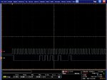
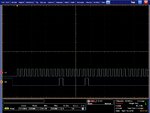
I used logic probes to see the output of the SCLK and SDIO pins (attached) and I don't see a problem. The SPI CS is permanently tied low.
I am not sure why writing to the registers does not work.
Here is the datasheet of the ADC since I couldn't upload the file:
https://www.analog.com/static/imported-files/data_sheets/AD9649.pdf
Any help/insight will be appreciated! Thanks.
The fpga clock is 48 MHz and serial clock for the ADC is 8 MHz. The VHDL code that I've written is given below.
Code:
LIBRARY IEEE;
USE IEEE.STD_LOGIC_1164.ALL;
USE IEEE.STD_LOGIC_UNSIGNED.ALL;
USE IEEE.NUMERIC_STD.all;

ENTITY SPI_MASTER IS
    GENERIC
    (
        NUM : INTEGER := 24
    );
    PORT
    (
        CLK_IN : IN STD_LOGIC;
        SPI_MASTER_SDIO : INOUT STD_LOGIC;
        SPI_MASTER_CLK : OUT STD_LOGIC;
        SPI_MASTER_CS : OUT STD_LOGIC;
        ADC_DATA_IN : OUT STD_LOGIC_VECTOR(7 DOWNTO 0)
    );
END ENTITY;

ARCHITECTURE BEHAV OF SPI_MASTER IS

    CONSTANT ADC_WRITE_REG : STD_LOGIC_VECTOR(12 DOWNTO 0) := '0' & x"008";             --WRITE REGISTER
    CONSTANT ADC_DATA : STD_LOGIC_VECTOR(7 DOWNTO 0) := x"10";                    --DATA TO WRITE

    CONSTANT ADC_READ_REG : STD_LOGIC_VECTOR(12 DOWNTO 0) := '0' & x"015";                --READ REGISTER

    SIGNAL DATA_TO_ADC : STD_LOGIC_VECTOR(NUM-1 DOWNTO 0) := '0' & "00" & ADC_WRITE_REG & ADC_DATA;

    SIGNAL DATA_FROM_ADC : STD_LOGIC_VECTOR(15 DOWNTO 0) := '1' & "00" & ADC_READ_REG;

    SIGNAL OE : STD_LOGIC := '1';                                     --OUTPUT ENABLE FROM FPGA, WHEN HIGH: SEND DATA TO ADC, WHEN LOW: RECEIVE DATA FROM ADC
    SIGNAL DATA_IN : STD_LOGIC_VECTOR(7 DOWNTO 0) := "11111111";
    SIGNAL MASTER_RST : STD_LOGIC := '0';
    SIGNAL SENT : INTEGER := 0;            --NUM BITS SENT
    SIGNAL RCVD : INTEGER := 0;            --NUM BITS RECEIVED
    SIGNAL ADC_CLK : STD_LOGIC := '0';        --SERIAL CLOCK FOR ADC
    SIGNAL COUNT : INTEGER := 0;

    BEGIN

        PROCESS(CLK_IN)
        BEGIN
            IF(RISING_EDGE(CLK_IN)) THEN
                IF(COUNT = 2) THEN
                    ADC_CLK <= NOT ADC_CLK;
                    COUNT <= 0;
                ELSE
                    COUNT <= COUNT + 1;
                END IF;
            END IF;
        END PROCESS;

        PROCESS(ADC_CLK,MASTER_RST,OE)

        BEGIN
            IF(FALLING_EDGE(ADC_CLK) AND MASTER_RST = '0') THEN
                IF(OE = '1') THEN
                    IF(SENT < 23) THEN
                        --DATA_FROM_ADC <= DATA_FROM_ADC(14 DOWNTO 0) & '1';
                        DATA_TO_ADC <= DATA_TO_ADC(22 DOWNTO 0) & '1';
                        SENT <= SENT + 1;
                    ELSE
                        OE <= '0';
                    END IF;
                END IF;
            ELSIF(RISING_EDGE(ADC_CLK) AND MASTER_RST = '0') THEN
                IF(OE = '0') THEN
                    DATA_IN <= DATA_IN(6 DOWNTO 0) & SPI_MASTER_SDIO;
                    RCVD <= RCVD + 1;
                    IF(RCVD > 6) THEN
                        MASTER_RST <= '1';
                    END IF;
                END IF;
            END IF;
        END PROCESS;

        --SPI_MASTER_SDIO <= DATA_FROM_ADC(15) WHEN OE = '1' ELSE 'Z';
        SPI_MASTER_CS <= '0';
        SPI_MASTER_CLK <= ADC_CLK;
        ADC_DATA_IN <= DATA_IN;
        SPI_MASTER_SDIO <= DATA_TO_ADC(23) WHEN OE = '1' ELSE 'Z';

END BEHAV;
The parts that are commented are used for reading from the ADC registers. Also when reading the "IF (sent < 23)" is changed to "IF (sent < 15)".
I used logic probes to see the output of the SCLK and SDIO pins (attached) and I don't see a problem. The SPI CS is permanently tied low.
I am not sure why writing to the registers does not work.
Here is the datasheet of the ADC since I couldn't upload the file:
https://www.analog.com/static/imported-files/data_sheets/AD9649.pdf
Any help/insight will be appreciated! Thanks.