Continue to Site

Welcome to EDAboard.com

Welcome to our site! EDAboard.com is an international Electronics Discussion Forum focused on EDA software, circuits, schematics, books, theory, papers, asic, pld, 8051, DSP, Network, RF, Analog Design, PCB, Service Manuals... and a whole lot more! To participate you need to register. Registration is free. Click here to register now.

resistor layout error. I am using generated pplyb resistor

Status
Not open for further replies.

jefffatt

Newbie level 3
Joined
Mar 24, 2012
Messages
4
Helped
0
Reputation
0
Reaction score
0
Trophy points
1,281
Activity points
1,309
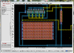
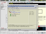
Hi, i am using silterra cmos 0.18um technology in my analog project. I am using ppylb as my resistor. I noticed from the schematic that the pplyb have three pins, however in the generated pplyb layout, it only have two contacts. After running LVS, I received a error saying that the nwell of the pplyb is floating or connected to multiple nets. Can I know what caused the errors? Thanks in advanced
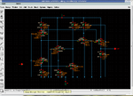
schematic.pngresistor layout.pnglvs check.png
 

At the schematic side you have connected the middle terminal of the resistor's symbol in gnd! .Connect it to vdd! instead,since as you say this type of resistor is implemented in nwell and then LVS again.
 

At the schematic side you have connected the middle terminal of the resistor's symbol in gnd! .Connect it to vdd! instead,since as you say this type of resistor is implemented in nwell and then LVS again.


Hi, thank for the reply. I had tried to connect the middle terminal to vdd! as you said, however it didnt solve the issue. Is it the layout of the pplyb is not correct? I am wondering why in schematic, the resistor have 3 terminals, but in layout generated, it has only 2 contacts.
 

You should also connect the nwell layer to vdd metal in your layout.Did you do that?

The third terminal of the device in your schematic represents the substrate or nwell connection based on where (sub or well) the device is manufactured.
 

You should also connect the nwell layer to vdd metal in your layout.Did you do that?

The third terminal of the device in your schematic represents the substrate or nwell connection based on where (sub or well) the device is manufactured.

Hi, really thanks for your reply. Is it just connect the middle terminal of the resistor to vdd!
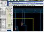
Like this?
new.png

I tried run LVS,however the issue still exists.
 

Almost yes...but you should place some (at least 2) nwell contacts in order to connect the nwell with vdd! with metal1.

More specifically,extend the nwell layer outside of the resistor's perimeter and put 2 nwell contacts in there,finally draw a metal 1 path from the contacts to vdd!
 

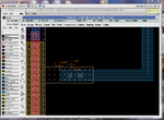
hi, may I know what is nwell contact? is it just an ordinary contact or others? I had tried to do what you taught me
test.png
however I received some DRC errors
i)Minimum poly overlap contact is 0.10um
ii)Minimum island overlap of contact is 0.10um
 

I think if you read your PDK manual you will solve the DRC errors and finally you must find a way to connect the nwell with Metal1 (try to find the correct name for nwell contact in your PDK manual or via the LSW window of Cadence,maybe
silterra gives a different name for this type of contact).
 

I think placing a p-tap around the resistor and connecting it to ground will solve the problem.


Thanks & Regards
Sreehari
 

Status
Not open for further replies.

Part and Inventory Search

Welcome to EDABoard.com

Sponsor

Back
Top