Continue to Site

Welcome to EDAboard.com

Welcome to our site! EDAboard.com is an international Electronics Discussion Forum focused on EDA software, circuits, schematics, books, theory, papers, asic, pld, 8051, DSP, Network, RF, Analog Design, PCB, Service Manuals... and a whole lot more! To participate you need to register. Registration is free. Click here to register now.

PWM to voltage conversion - OpAmp offset.

Status
Not open for further replies.

vojtik

Newbie level 4
Joined
Mar 7, 2012
Messages
5
Helped
0
Reputation
0
Reaction score
0
Trophy points
1,281
Activity points
1,326
Hi all.
I'm strugling with PWM to voltage converter. PWM duty 0-100%, ampl. 5V, freq.300Hz-3kHz. PWM signal is produced as High Side Driver (pull down resistor at converter's side). Current capability up to 2mA .

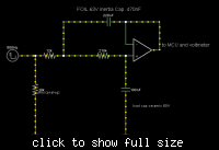
Please help me to debug the following circuit which is supposed to convert PWM to voltage (there can be also 0-5V voltage at the input to the circuit- in this case the circuit must serve as voltage follower ).


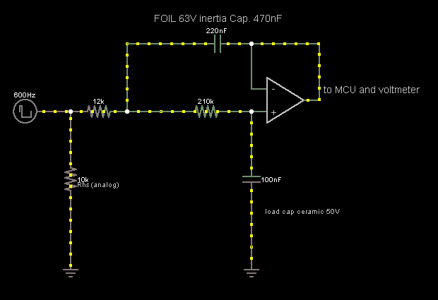
The circuit should be working well (tested by a friend of mine) with Opamp LMC662CN used with unipolar supply (https://uk.rs-online.com/web/p/op-amp/5344232/). Anyway, I'm not able to make a test as I dont have this OpAmp.

I was forced to used OpAmp TLC271, supplied with unipolar 12V. This is not a rail2rail kind but should it mind when high Vdd used?!
In simulation works quite fine.
Reality differs. The voltage following is ok.
PWM to voltage conversion is NOK. the difference is huge (50%PWM is not 2.5V but about 2.63V, 10% PWM is about 0.7V and not the expected half volt). Vcc always 5V+/- 0.002V.
I'm already desperate and dont understand why there is the offset. ANy thoughts why LMC662 works and TLC271 doesn't? Any important parameter I overlooked? Please could any of you propose an alternative OpAmp which would work and explain why.
Thanks a lot.
 

The offset is large enough to locate it's origin in a thorough measurement. I don't see an obvious explanation. Besides possible instability of the OP stage, e.g. brought up by excessive capacitive load, I suspect the digital driver. Can you please tell details about the implementation? As a simple test, what's the behaviour with DC input?

As a side remark, the active filter dimensioning is far from a reasonable second order filter prototype. For fast settling with optimal PWM suppression, a Butterworth (small overshoot) or Bessel filter (effectively no overshoot) seems suitable.
 

atmega_ADC_circuit.PNGThanks. The output goes directly to Analog input pin of an Atmega8 MCU.
With the DC input the output is exactly the same as input (+/2mV) so works well with DC.
Anything i can diagnose? Have a limited equipment (about 10kHz probe, no oscilloscope at the moment)
I overtook this circuit from an existing design w/o changing anything else than the OpAmp. Honestly i dont know much about filter designs so appreciate all your suggestions regarding the correct values.
 

There should be no capacitive load in this case. The DC test refers to possible switching speed or leakage problems of the digital output supplying the PWM.

For the filter dimensioning, you need to specify either the acceptable residual PWM ripple or the settling time. Or both, and check if it's feasible with a 2nd order filter.
 

Guys, I checked once again the circuit. It's correct. Also tried to play with the C1,C2 and resistor values according to different designs in Microchip FilterLab.
Used a different piece of TLC271...and no success. No more ideas why this doesn't work.
 

As long as you don't give any infomation about the driver side, I stay with my respective guesses.
 

PWM driver information I have: HSD type, output has 4.7nF to GND, VCC has 220nF to GND at driver side.
For RHS reccomended values: 1k5 ... 20 kΩ
 

How about a type specification?

To ask the other way around: What makes you think that the PWM driver is proving sufficient linearity in duty cycle to voltage conversion?
 

The TLC271 is a low power op amp. It does not like your 0.2 or 0.5uF capacitor as a load. It's oscillating. Either make R's 10-20 times larger and C's 10-20 times smaller, or depending on how much attenuation you actually need, just go R-C R-C 12k, with 0.2uF to ground feeding 210k with 0.1uF to ground, then your follower.
 

The TLC271 is a low power op amp. It does not like your 0.2 or 0.5uF capacitor as a load. It's oscillating.
Are you referring to the active filter circuit? I can't see an involved stability problem. The filter capacitor doesn't represent a critical capacitive load to the OP output due to the resistive part. Loop stability of the second order filter can be a problem in general, but it shouldn't with the present (unreasonable) low filter Q.

Stability can be of course thwarted by a capacitive output load, but the OP claimed that there's none.
 

FvM - you're right; the 12k is high enough that even the low bias version of the 271 should be ok. Can you put a schottky diode to parallel RC on the output to hook your meter to? We might be able to catch oscillation on the output (the D-R-C will be a peak detector) that you can see with your voltmeter. One more thought - remove the feedback C and see if the output still messed up.
 

Thanks for the hints. I'll try and let you know. First of all must change the MCU that passed away during the last experiments.
 

I thought of something last night. Any chance it's the PIC doing something to the opamp output? Can you cut the trace and insert a 1k resistor going into the A/D converter input? (Unless you've already tried it without the PIC in circuit). That way you can see if there is a voltage difference between the opamp and the PIC.

Do you know why the PIC died? Circuit problem or operator error?
 

Status
Not open for further replies.

Similar threads

Part and Inventory Search

Welcome to EDABoard.com

Sponsor

Back
Top