Continue to Site

Welcome to EDAboard.com

Welcome to our site! EDAboard.com is an international Electronics Discussion Forum focused on EDA software, circuits, schematics, books, theory, papers, asic, pld, 8051, DSP, Network, RF, Analog Design, PCB, Service Manuals... and a whole lot more! To participate you need to register. Registration is free. Click here to register now.

Help me identify failure mode of RF FET

Status
Not open for further replies.

mtwieg

Advanced Member level 6
Joined
Jan 20, 2011
Messages
3,835
Helped
1,310
Reputation
2,626
Reaction score
1,405
Trophy points
1,393
Activity points
29,370
Hello, I'm trying to build a current mode class D amp at ~8MHz, ~50W out. For this I'm trying to use the MRF1518 FET, but when I try to bring the power beyond a certain point, they always fail in the same way. I'll describe in detail what I'm doing.

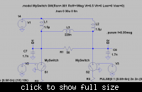
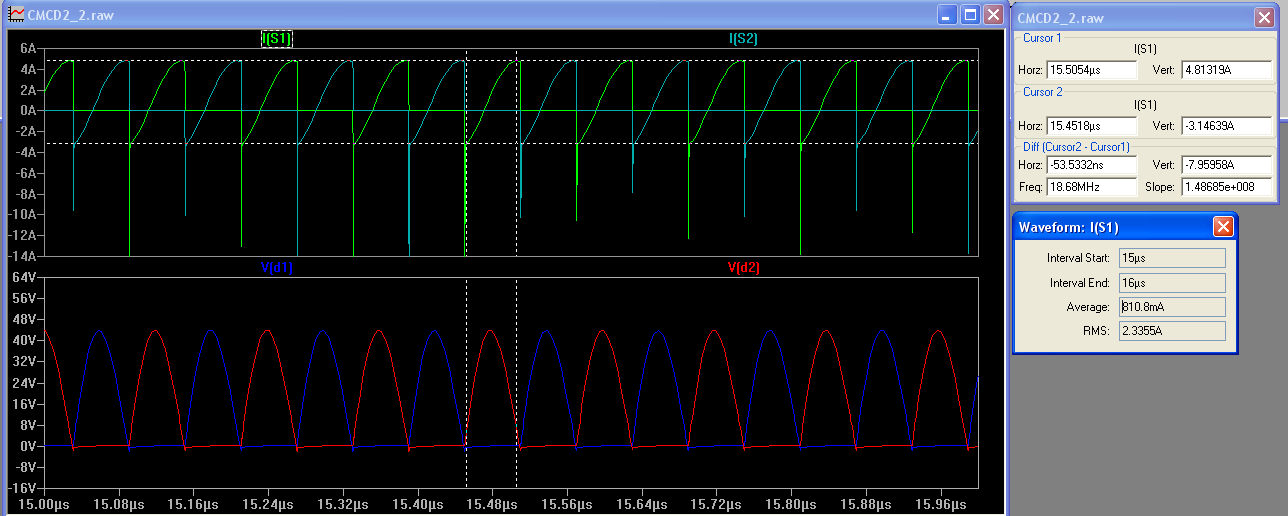
Here's a rough schematic in LTspice of a low power tuning of the amp. The FETs are modeled as ideal switches (can't find an actual model to import, and it works well enough I believe) driven 180 degrees out of phase. In reality they are each driven by class E amps, with about 20Vpp on the gates. The L and Cs are chosen to give zero voltage switching. The load here is 50ohms. In the case the amp works fine, and I've taken the supply voltage up to 14VDC (about 18W out). Nothing heats up noticeably.

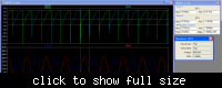
Here are the simulated waveforms of the FET drain currents and drain voltages. The boxes on the right show the max, min, RMS, and average of the drain currents.


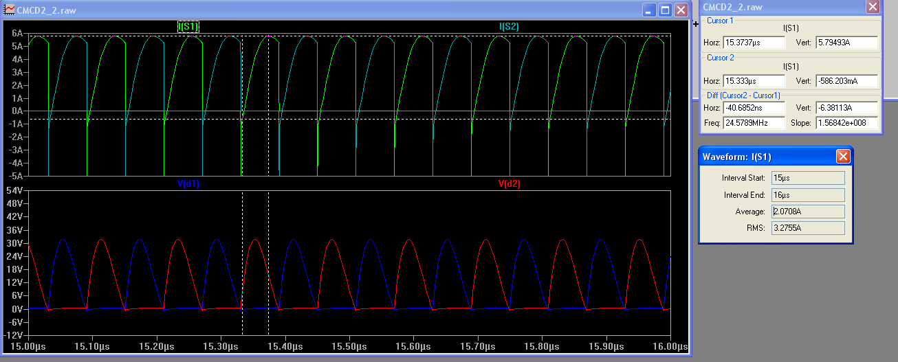
Now I try to step up the power by dropping my load impedance to 12.5ohms (done in reality with 1:4 impedance transformer). I retune the L and Cs a bit to maintain good zero crossings. But now whenever I try to take the supply voltage above around 10V, one of the MOSFETs will fail. Here's what the waveforms look like under those simulated conditions.

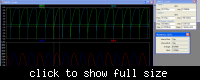
So the actual currents aren't incredibly higher. The failures happen even when doing short (like 30us), non repetitive bursts of operation. Prior to bumping the supply voltage past 10V, the devices are completely cool. The datasheet for the devices is pretty vague when it comes to giving max ratings. It merely states the max "continuous DC current" is 4ADC, and that total device dissipation is limited to 62.5W (definitely not violating that limit...). When the failure happens, the peak drain voltage (that I can observe) is less than the rated breakdown voltage, and it's much less than it was during the first test (in which the load was 50ohms and the supply was 14V). The peak gate voltage is also less than the max rating (+/-20V).

When one of the FETs fails, its gate-source resistance always appears low, normally between 10 and 200ohms. Often the FET will still apparently work, though not nearly as well. This is always the case, and I've gone through about 6 FETs like this.

Does anyone have any ideas on what might be causing this sudden failure? Is there some physical phenomenon that just limits the peak current that I can push through the device, even for very short periods of time. If I change devices, how can I get more bang for my buck?
 

You say in your second paragraph that you are putting 20V p-p on the gates (although you later say peak gate voltage is less than that). It sure SOUNDS like you are damaging the gate of the device. Perhaps there's some parasitic capacitance that's causing the VGS to exceed 20V. Have you looked at Vgs with a scope?
 

Have you cracked a failed FET open to see where and what the failure was?

It might require dissolving the plastic depending on the part; on the old Motorola J-Zero packages in the past is was just a matter of heating the package and the ceramic cap would come off to examine the failure (like bond wire pop or small explosion in the base-emitter area).

From the sounds of it, you might have violated Gate-Source breakdown voltage limits.

Jim
 

You say in your second paragraph that you are putting 20V p-p on the gates (although you later say peak gate voltage is less than that).
Yes, 20V peak to peak, so 10V amplitude, which is much less than the device is rated.
It sure SOUNDS like you are damaging the gate of the device. Perhaps there's some parasitic capacitance that's causing the VGS to exceed 20V. Have you looked at Vgs with a scope?
Yes, the VGS doesn't really change at all due to different loading or different supply voltage. It never goes above 12V.

Previously I was driving the gates with less voltage (about 8V max), and I was still getting the same failures at the same load. I tried increasing it since I thought the problem might me that I wasn't switching it on hard enough, but it didn't change anything.

Have you cracked a failed FET open to see where and what the failure was?

It might require dissolving the plastic depending on the part; on the old Motorola J-Zero packages in the past is was just a matter of heating the package and the ceramic cap would come off to examine the failure (like bond wire pop or small explosion in the base-emitter area).

From the sounds of it, you might have violated Gate-Source breakdown voltage limits.

Jim
I don't think I have the resources (chemicals, microscope, etc) necessary to really inspect the device dies. And I'm not really sure what I'd look for anyways.

I can't see how I could possibly be exceeding the Vgs limit. Even if there is some internal gate inductance, how could the gate internally get pulled up by an extra 10V or so, especially at such a low operating frequency? And what would that have to do with the load current?
 
Last edited:

Is it possible you're getting some inductive kick from those 1.5uH devices? That could be coupled through the drain-gate capacitance. (And keep in mind, frequency has nothing to do with it, it's edge-rate)
 

L3 220 n ???
what is the fet model ?
u will need diodes on l1 l2 or checkout if the fets have internal diodes.
i assume u want to pass current thru load r1, so what kind of pulse u expect to get on r1 ?
if u know ltspice send the asc file .
 
Last edited:

Is it possible you're getting some inductive kick from those 1.5uH devices? That could be coupled through the drain-gate capacitance. (And keep in mind, frequency has nothing to do with it, it's edge-rate)
Okay, so the rising edge is around 2.5V/ns, and the reverse transfer capacitance is 4.5pF according to the datasheet, so that gives about 11.5ma from drain to gate. The impedance at the gate is <50ohms, so that could only induce about 0.1V of extra voltage. Even with some series inductance the induced voltage won't be very high. And that rising edge occurs right around when the device enters cutoff (Vgs is between 1-2V), so it would take a huge kick to kill the gate at that time. I don't see it happening.

L3 220 n ???
what is the fet model ?
As I said the FET is a MRF1518. The datasheet is here: **broken link removed**

u will need diodes on l1 l2 or checkout if the fets have internal diodes.
They do have diodes but they shouldn't be used in this topology, since the switches only conduct when Vgs is high.
i assume u want to pass current thru load r1, so what kind of pulse u expect to get on r1 ?
if u know ltspice send the asc file .
The forum attachment manager doesn't seem to like .asc files....

edit: here I've attached a zipped version of the .asc file:
View attachment CMCD2.zip
 
Last edited:

index
that's what u are really doing ?
 

What rising edge are you refering to? I'm thinking, you've got some current flowing through the 1.5uH, and then you turn off the MOSFET.

V=L *di/dt.

Let's say you've got 10V across that 50 ohms-->200mA. Now, say that fet turns off in 2 nS (I'm just throwing numbers out). That means you've got:

V=1.5uH*0.2/2ns=150V. !!

Even if the FET turns off in 20nS, you're going to get a 15V spike. I'm just sayin'. (This is the kind of situation where you might not see the effect because your scope probe kills it).
 

index
that's what u are really doing ?
No, not really. The supply chokes are not coupled together, and are just meant to supply a roughly constant current to the amplifier drains.

What rising edge are you refering to? I'm thinking, you've got some current flowing through the 1.5uH, and then you turn off the MOSFET.

V=L *di/dt.

Let's say you've got 10V across that 50 ohms-->200mA. Now, say that fet turns off in 2 nS (I'm just throwing numbers out). That means you've got:

V=1.5uH*0.2/2ns=150V. !!

Even if the FET turns off in 20nS, you're going to get a 15V spike. I'm just sayin'. (This is the kind of situation where you might not see the effect because your scope probe kills it).
No, this doesn't happen because during turn off the current in the inductor is diverted into the drain-source capacitor, which leads to soft switching behavior. Of course there is internal inductance inside the FET, but there is also internal capacitance, which means the slew rate, and the peak voltage, at the drain is well defined, and should be well within the device capabilities.
 
Last edited:

I don't have much experience of this variant of class D but the first thing that jumps out at me looking at your simulation is you have the potential for very high common mode gain around 3MHz. i.e. I'd expect to see a very sharp spike of common mode gain and this could cause problems?

Obviously, your simulation won't demonstatrate this issue because your driving source is perfectly differential but in the real world you could get instabilty at 3MHz?

Can you try fitting your filter capacitance across the 220nH inductor rather than in shunt? i.e. change the 1.7nF caps?

I'm not sure what this does for common mode resonances but you would at least lose the huge spiky common mode gain at 3MHz...
Putting the resonant capacitors in parallel with the 220nH inductor does work well in theory, but in practice this gives rise to undamped resonance between the parasitic drain inductance of the FETs and their drain capacitance. This creates some nasty waveforms. Putting the capacitance in parallel with each drain helps greatly to dampen the ringing.

The resonance formed by the 1.5uH chokes and the resonant caps is heavily damped by the load resistance (when the amplifier is driven at resonance, anyways). It's somewhat of a concern when trying to quickly modulate the supply voltage, but I'm only varying it very slowly now, so it shouldn't be a problem; at least not for the FETs.
 

The other thing to try on your existing circuit would be to try fitting 2200 ohm resistors across the 1.5uH chokes. This would damp the Q of the 3MHz common mode resonance at the expense of a small amount of efficiency.

---------- Post added at 00:27 ---------- Previous post was at 00:18 ----------

The resonance formed by the 1.5uH chokes and the resonant caps is heavily damped by the load resistance (when the amplifier is driven at resonance, anyways). It's somewhat of a concern when trying to quickly modulate the supply voltage, but I'm only varying it very slowly now, so it shouldn't be a problem; at least not for the FETs.


if you strapped both gates together and drove them from an AC source and did an AC analysis I'd expect to see lots of common mode voltage gain at 3MHz. I don't see how the load can damp this type of gain?

Hence the suggestion to try the 2200 ohm resistors?

However, I guess you would have seen instability on a scope etc. I was concerned in case your 'real' circuit could squeg at 3MHz. i.e. the problem could be how you couple up the driver circuit because it could introduce a common squeg mode.

Also I'm assuming your RF layout is good with short connections to the 1.7nF caps and the drain/inductors and you are using good quality components.

I'm afraid that's all I can suggest. Good luck :)
 
Last edited:
  • Like
Reactions: mtwieg

    mtwieg

    Points: 2
    Helpful Answer Positive Rating
if you strapped both gates together and drove them from an AC source and did an AC analysis I'd expect to see lots of common mode voltage gain at 3MHz. I don't see how the load can damp this type of gain?
Correct, when driven with common mode signals (either on the gates of the FETs or on the supply voltage) there will be a resonance there. The reason it's damped by the load, even though the load is differential, not common mode, is that when the FETs are driven at the correct frequency and 180 out of phase (as they should), the load effectively becomes common mode (since it is always shorted to ground at one end). And that dissipation will be proportional to the drain bias voltage, thus making it act like a linear damping function. So long as the FETs are operating, the load will dissipate common mode signals.
Hence the suggestion to try the 2200 ohm resistors?

However, I guess you would have seen instability on a scope etc. I was concerned in case your 'real' circuit could squeg at 3MHz. i.e. the problem could be how you couple up the driver circuit because it could introduce a common squeg mode.

Also I'm assuming your RF layout is good with short connections to the 1.7nF caps and the drain/inductors and you are using good quality components.

I'm afraid that's all I can suggest. Good luck :)
I tried damping resistors and didn't see any difference. It was worth a try though.

I think the only options left are either some bizarre transient behavior at the start or end of my RF pulse (I do this by pulling the gate bias on the FETs to either -5V or +1.2V, and gating the gate drive waveforms), or there is just some bizarre limit on drain current in the device.


Anyways, I have another related question. I eventually want to try doing this topology at higher frequencies (like 100MHz or more), but when doing that it becomes necessary to shrink that resonant inductor, to the neighborhood of 10nH or less. At that point I'm wondering if microstrip or stub components would be a better way to implement that inductor? I don't really have any experience with regards to microstrip filters, especially with differential loads like that. Any recommendations?
 

Ok
Why r u using marginal 1v (min from data ) for gate u may slide into grey area of linear area instead of switch ?
check out vdss value (gate off)is higher than regular vds = 12.5v.. ltspice show u have 27v
di d2 did not understand r they or not in circuit and how ?
 

Ok
Why r u using marginal 1v (min from data ) for gate u may slide into grey area of linear area instead of switch ?
It's important that the FETs are hard switched, that's how you get good efficiency. The bias voltage on the gate doesn't really change how linear the FETs operate, but it does effectively adjust their duty cycle.
check out vdss value (gate off)is higher than regular vds = 12.5v.. ltspice show u have 27v
di d2 did not understand r they or not in circuit and how ?
I'm not sure what you're referring to here... are you talking about the gate threshold voltage changing with Vds? And the diodes are not in the circuit because they wouldn't have any effect (unless the circuit was severely detuned).
 

Status
Not open for further replies.

Part and Inventory Search

Welcome to EDABoard.com

Sponsor

Back
Top