Continue to Site

Welcome to EDAboard.com

Welcome to our site! EDAboard.com is an international Electronics Discussion Forum focused on EDA software, circuits, schematics, books, theory, papers, asic, pld, 8051, DSP, Network, RF, Analog Design, PCB, Service Manuals... and a whole lot more! To participate you need to register. Registration is free. Click here to register now.

copper pour small gaps Altium

Status
Not open for further replies.

tweekzilla

Newbie level 6
Joined
Oct 12, 2011
Messages
11
Helped
0
Reputation
0
Reaction score
0
Trophy points
1,281
Activity points
1,369
Hi,

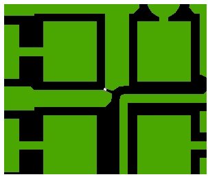
I'm doing a final copper pour (no net connection) to the top and bottom of a 6-layer board in Altium. The copper pour tends to leave small feature (gaps) as seen below no matter how much I tune the pour algorithm. These gaps then get flagged in freeDFM for advanced circuits - Some questions:

1) Do these small gaps really matter in manufacture when it's an unconnected copper plane?
2) Is there a way in Altium to get it to recognize these errors in the design check? It doesn't seem to care about them and I'd rather not have to upload every time to check for these gaps
3) Is there a way to stop Altium from leaving these gaps when doing the pour?

Thanks!

Ross

28_1328628078.jpg
 

Thats why we need to use DFM software untill the functions are built into the PCB software.
PCB software is looking for electrical DRC problems, DFM is looking for PCB fabrication problems.
Put a very small chamfer on the track next to the pad and you'll get rid of that gap.
 
you should play around with the polygon pour setting. Especially with the "Remove Islands less than" and "Remove necks when copper width less than".
You can also increase the clearance between the polygon and all other copper objects.

You may want to connect that copper to something (GND or CHASSIS or other net). It is bad practice to float the copper.

Thanks for the reply - I've been going backwards and forwards as to whether or not to flood the top and bottom layers with copper. I've read in places that it's fine to have it floating and in others not. I don't want to connect it to GND as I already have an internal GND plane and CHASSIS scares me a little give my overall grounding scheme (thinking GND loops and other nasties). If there really is no benefit from flooding the top and bottom then I can just get rid of it and problem solved - Note that this is all pretty low frequency stuff on there. I'm just trying to eliminate noise pickup

---------- Post added at 11:48 ---------- Previous post was at 11:47 ----------

[/COLOR]
Thats why we need to use DFM software untill the functions are built into the PCB software.
PCB software is looking for electrical DRC problems, DFM is looking for PCB fabrication problems.
Put a very small chamfer on the track next to the pad and you'll get rid of that gap.

Yep I can just cut back the copper in the regions where it's fouling. I'm being lazy and trying to get the software to do it for me :) Thanks for the advice!
 

If you have ground planes already in the board,then the copper pour will not do much in anything. It will change the impedance of the traces that have pour near them. And small floating copper areas will act as a small antennae.
It would be OK if it is a high impedance analogue design with only 2 layers. And then you would connect the pour to GND.

Ok I think I just won't do the copper pour on the top and bottom layers.
 

I always pour copper on top and bottom layers with lots of stiching vias connecting the copper to GND. I would say from the designs I see that this is standard practice. When going to HDI design this is taken one step further with all the top and bottom layer being a ground pour, with just holes where the pads are.
 
Status
Not open for further replies.

Part and Inventory Search

Welcome to EDABoard.com

Sponsor

Back
Top