Continue to Site

Welcome to EDAboard.com

Welcome to our site! EDAboard.com is an international Electronics Discussion Forum focused on EDA software, circuits, schematics, books, theory, papers, asic, pld, 8051, DSP, Network, RF, Analog Design, PCB, Service Manuals... and a whole lot more! To participate you need to register. Registration is free. Click here to register now.

driver for power mosfets of 1 kV half bridge power supply

Status
Not open for further replies.

arkanwe

Junior Member level 1
Joined
Mar 23, 2011
Messages
17
Helped
1
Reputation
2
Reaction score
1
Trophy points
1,283
Activity points
1,449
Hello, how are you?

I'm trying to design a high voltage power supply. It's the first SMPS I try to do. I've chosen a switching DC-DC converter,Half-Bridge, with the IC TL494 for control. The specifications are:
Vin = 311 V
Vout = 1 kV
Fsw = 55 kHz
Iout = 0.1 A

So far I came out with the following schematic,
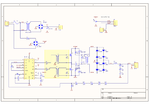
SMPS_HB_01.png

The trouble is, how to drive the power mosfets?. I can't buy IC mosfet drivers, so it has to be with transformers.
I've seen circuits with many components on the gate side(R,C, & D), and different connections for the driver transformer side, with additional transistors.

The way it is I think it will either not switch, oscillate the gates, or make a short circuit on the mosfets. What do you think?

Can you recommend me what to do, schematic or book, to learn about this kind of problem?
It would be great to find some literature with a good explanation about this kind of problems, and topology.

Also, I'm missing line filter parts, over load protection, and maybe other important things, typical on ATX power supplys. But, I'm just starting with this, and only need a simple power supply working and reliable. Is there something really really important missing??

I didn't tested it as is yet, have fear to blow all up :-S

Many thanks in advance
 

Dear arkanwe
Hi
At first step , i should say , i don't suggest you to make this circuit if it is your first time with SMPS . because at this voltage you should know many things . it is very simple to build . but it can be dangerous for you . by the way , did you read about SMPS , until now ?
Best Wishes
Goldsmith

---------- Post added at 21:43 ---------- Previous post was at 21:40 ----------

BTW : do you know , that 1n4007 ins not ok for your purpose , because you want drive it with 50KHZ!!!!!!!!!!!!! and 1n4007 is not good for this aim . at first step you should try to make some switching circuits with lower voltages . and then after earning some experiences , you can do it simply .
 

Hi Goldsmith, thanks for answer!
It's very wise from you to warn me about this project; it is dangerous.

Recently I've been working with 700V linear circuits, and have some experience with burning resistors, exploding components, and electric arcs on pcb tracks before success,...nasty things... Also tested a push pull smps design from the internet, but of 500V, and it worked fair enough..

I've studied SMPS from a book, some ATX schematics, and internet. That's how I came up with this schematic. But I'm still missing information about the transistor drivers on this topology, and how to properly design a switching transformer. I'm unsure because it's the first smps project I do from scratch and of high voltage.
Between a power electronics book, and a typical ATX PSU schematic, there is a big gap to fill.

You're totally right about the diodes, I forgot to use an ultra fast diode like UF4007

Thanks again, best regards
 

Dear arkanwe
Read These two terrific and practical book : switching power supply design of professor abraham i pressman and switching power supply cookbook of professor marty brown.
By the way , the distance between two high voltage pins , at 50HZ , instead of each KV , at least should be about 1 mm . but when the frequency increased , you should , pay more attention.

Good luck
Goldsmith
 
I've just checked the index of the pressman book and it looks like just what I need, it's much interesting than other books I've read.
I'll try to advance on this, thank you very much goldsmith!
 

Hello again.
So I've built the power source. It's an half bridge, from 220AC to 1kV DC. Switching at 200kHz. Control is done with a TL494.
It was designed for a load of 100mA. With no load works OK! I can adjust the V output from 0 to 1100 V.
The transistors get little hot, but it's ok, I've put a fan.

But!, when I tested it with about 10 mA , the output voltage immediately drops down to near 500V.
The input to the transformer is +- 155V. The turns ratio is n=10 aprox. The windings were done with wire AWG35.
R_primary=10 ohm. R_secondary = 100 Ohm.
C filter output = 3 capacitors 10uF/450V in series. L filter output = 20 mHy aprox.

Any idea why this could happen? What should I try??

(I've already re-done the windings)
 

Dear arkanwe
Hi
That drop has some meaning :
1- your out put inductor hasn't gap space or enough gap space . ( create enough gape space at it's core.)
2- ESR of your capacitors ! as i saw , you used 3 cap in series together thus , you'll have summation between , three ESR .

And remark : i think you can take your feed back with an opto coupler to provide isolated out put .
Best Wishes
Goldsmith

Cool!
mmmhh, I've forgot the ESR... I'll check that...
What do you mean with gap space? I've used a toroid from the output of a old atx....
Thanks!!!
 

Hi arkanwe
ESR ( equivalent series resistor )( each capacitor has an internally resistor that is due to the rolling ).
And about Gap space , as we know , the core of each inductor can works at linear or nonlinear region . and to avoiding from core saturation and preventing from nonlinearity , we should create enough gap space on core . as i can remember , some years ago i designed a buck regulator . and when i putted a load on the out put , the voltage immediately , decreased , and when i used a gapped core , (air gap ) the problem solved , simply ! and after that time all of my ferrite cores at DC signal or complex signal , has gapped core .
Best Wishes
Goldsmith
 

hello goldsmith
where can i get this gapped core
 

Dear Hz2020
Hi
You can buy a core without gap and create enough gap on that ( if you use toroidal core it will be very hard to rift that with saw ! but if you buy PQ or other E type cores , you can do it very simple .) but there is another option to buy gapped core from inductor sellers .
Good luck
Goldsmith
 

You shouldn't be using gate drive transformers in a half bridge supply. It is nearly impossible to prevent saturation while maintaining a good output voltage. There are methods for making GDTs work for applications like these (where a wide range of duty cycle is necessary), but they are pretty advanced and cause huge problems if not implemented correctly. Your gate drive transformer, as shown on the schematic, is also pretty poor. You need a DC blocking cap on the primaries. The 220ohm series resistor is also way too high, try something in the range of 5-20ohms. And the gate pulldown resistors should be much higher (>10Kohm).

I have to strongly advise you get a proper high side gate driver, or choose a topology which doesn't need one. For your power levels, you don't even need something as sophisticated as a half bridge topology. A simple flyback or forward converter would probably work fine, or a diagonal flyback/forward converter (which has high side switches which can be used with GDTs).
 

Again Hi
Yes i'm agree with mtwieg . you should use a capacitor in series with primary and then at secondary using and RCD network . it will be better .
Best Regards
Goldsmith

---------- Post added at 19:16 ---------- Previous post was at 19:15 ----------

BTW : the series resistance for gate is needed and the value of parallel resistor is low and you can increase it up yo 47 k.( as mtwieg said)
 

TL494 need a refference voltage on pin 2. Connect Vref to pin 2 direct or by a divisor. TL494 have Vref = 5V. If pin 2 is direct connected to Vref (5V), voltage to pin 1 must be according arranged to be arround 5V for nominal output voltage. R6 must be increased to 6.1k. Also include a capacitor in feedback loop (10nF in series with R6.
 

Hello again everybody!. Thank you for all the interesting comments and suggestions, very cool!

Here is the actual circuit schematic tested.
Please!!!, pay attention with the net names, some of the nets are linked by name, not by a line draw.

**broken link removed**

The problem now is this. The load is moderate (20mA at 800V). Set the VCTRL to start with voltage at 0V. With the trim pot I change the reference voltage, to go up. Going up, "steady as she goes", to about 550V. Then, it suddenly drops to 500V and stays there fixed. And delivers current to the load circuit.

With no load it can reach 1000V and more. With a load of 200 kOhm(5mA) also works OK. Has 5V of ripple.

The thing of the gapped core is interesting...I'll try that. I thought the output inductor has to do only with the signal quality, the ripple, just a filter for AC. And never thought it will saturate with such low current. From calculations the flux density should be lower than 0.1 T (or 1000G) on that core, which is a low B for ferrite right?

I've used a half bridge topology because the high voltage levels on primary and specially secondary. I thought that the transistors will be fatally stressed by the voltage peak during the off on the primary of the flyback.

The gate drivers work fairly well. Could be better, shure, but I don't want put it more complex. They are very similar to the ones you can find on a ATX power supply. Maybe it's a good idea to lower R21 from 220Ohm to...22 Ohm.

Of course it lacks from short circuit and over current protection. It's necessary to put an Schmitt trigger, feedback from output and transistors but, that comes later.

Best regards!
 

Here is the actual circuit schematic tested.
Please!!!, pay attention with the net names, some of the nets are linked by name, not by a line draw.

**broken link removed**
The attachment isn't working, try again.
I've used a half bridge topology because the high voltage levels on primary and specially secondary. I thought that the transistors will be fatally stressed by the voltage peak during the off on the primary of the flyback.
High transistor stress is a good reason to use a half bridge design in some cases, but there are other topologies (like diagonal half bridge and flyback) which also have this benefit, and are able to work properly with gate drive transformers. Half bridge only makes sense if you're working with high power levels and want optimal transformer sizing, but you're only working with 100W, so half bridge isn't necessary.
The gate drivers work fairly well. Could be better, shure, but I don't want put it more complex. They are very similar to the ones you can find on a ATX power supply. Maybe it's a good idea to lower R21 from 220Ohm to...22 Ohm.
Your gate drivers shouldn't work well by design. You're losing half your drive voltage in those resistors, and the one with a higher duty cycle will have further reduced drive voltage during its on period. If, as you said before, your FETs are getting warm with no load on the output, then you have a problem and that gate drive circuitry is definitely part of it.
 

Dear mtwieg
Hi
What is "diagonal half bridge " ? i'm not familiar with that and what is the difference between that and a usual half bridge ? ( with simultaneous supply or with single supply and two capacitor ) ?
Is it possible that you tell me about it , please ?
Best Regards
Goldsmith
 

Dear steveelliott
Hi
Thank you very much for your attention , yes i'm familiar with forward converters .
Best Regards
Goldsmith ;-)
 

Yes, when I say diagonal I basically mean two-switch. There are two-switch/diagonal versions of both forward and flyback converters (not half bridge, which inherently has two complementary switches), which have the advantage of reducing voltage stress on the transistors and reducing losses due to leakage inductance vs single switch flybacks/forwards.
 
Status
Not open for further replies.

Similar threads

Part and Inventory Search

Welcome to EDABoard.com

Sponsor

Back
Top