Aytan
Newbie level 4
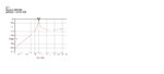
i am designing Narrow band Inductive Source Degenerated LNA using NMOS and 90nm mode using adsl. i am getting proper the frequency response at 2.4GHz for s(2,1) plot but the gain is negative. i don't knw what could be casing the gain to negative. i have attached the plot both as .dds and .jpg and also the schematic of the circuit and the model. can anyone please explain to me what causes the gain to be negative? thanks