mmitchell
Advanced Member level 4
Hi,
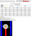
IPC-2221 Table 6-1 (page 51) defined conductor clearance for internal and external layers and different coating conditions. For B-1 (Internal Conductors) class, the description (highlighted in red) says it is also applicable to conductor-PTH spacing.

However, there are still {B2, B3, B4, A5, A6, A7} classes:
For which in descriptions following, no particular words have been given on whether they also apply to conductor-PTH spacing.
Are Table 6-1 columns for columns other than B1 applicable to conductor-PTH spacing?
I am asking this because of the case showing in the lower part of the attached image: How far should I separate a via’s hole with tracks in same and different nets, only considering the separation between track and hole alone, not including via land (annular ring) at the time being?
Matt
IPC-2221 Table 6-1 (page 51) defined conductor clearance for internal and external layers and different coating conditions. For B-1 (Internal Conductors) class, the description (highlighted in red) says it is also applicable to conductor-PTH spacing.

However, there are still {B2, B3, B4, A5, A6, A7} classes:
- B2 - External Conductors, uncoated, sea level to 3050 m
- B3 - External Conductors, uncoated, over 3050 m
- B4 - External Conductors, with permanent polymer coating (any elevation)
- A5 - External Conductors, with conformal coating over assembly (any elevation)
- A6 - External Component lead/termination, uncoated
- A7 - External Component lead termination, with conformal coating (any elevation)
For which in descriptions following, no particular words have been given on whether they also apply to conductor-PTH spacing.
Are Table 6-1 columns for columns other than B1 applicable to conductor-PTH spacing?
I am asking this because of the case showing in the lower part of the attached image: How far should I separate a via’s hole with tracks in same and different nets, only considering the separation between track and hole alone, not including via land (annular ring) at the time being?
Matt