Continue to Site

Welcome to EDAboard.com

Welcome to our site! EDAboard.com is an international Electronics Discussion Forum focused on EDA software, circuits, schematics, books, theory, papers, asic, pld, 8051, DSP, Network, RF, Analog Design, PCB, Service Manuals... and a whole lot more! To participate you need to register. Registration is free. Click here to register now.

“Courtyard Manufacturing Zone”?

Status
Not open for further replies.

mmitchell

Advanced Member level 4
Joined
Dec 3, 2011
Messages
107
Helped
0
Reputation
0
Reaction score
0
Trophy points
1,296
Activity points
2,203
Hi,

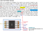
In IPC-7351 there is the concept of courtyard, courtyard excess, and courtyard manufacturing zone. I don’t understand what “courtyard manufacturing zone” is:
  • “Courtyard excess” already defined the amount of protrusion.
  • But why in Fig. 3-5 “courtyard manufacturing zone” seems to add another round of protrusion outside “courtyard excess”?
Courtyard_Manufacturing_Zone.png


Matt
 
Last edited by a moderator:

**broken link removed**

PDF page 23 Section 10.3
 
Last edited by a moderator:
Marce,

I have read your link to The CAD Library of the Future by Tom Hausherr, however I still don’t understand what “courtyard manufacturing zone” is.

In IPC-7351, table 3-4 to table 3-14 provide courtyard excess value for all types of packaging. However, not a single numeric value can be found at all for “courtyard manufacturing zone”.

It’s the Courtyard Manufacturing Zone that is critical for the assembly process. This is the Body-to-Body clearance that you set in your Design Rules for Design Rule Checking. The size of the manufacturing tolerance must come from the assembly shop that is going to be used to populate the parts on the PC Board. Every assembly shop has different assembly tolerances, but the average is 0.1mm.

Could “courtyard manufacturing zone” be zero? Is it totally dependent on manufacturer’s facility? Why no value is provided in IPC-7351?

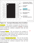
courtyard_mitzner.png

I am also attaching another screenshot from Kraig Mitzer’s Complete PCB Design Using OrCAD Capture and PCB Editor, page 89. I think his illustration is much clearer, but why he doesn’t include “courtyard manufacturing zone” in the drawing, but only with “courtyard excess”?


Matt
 

Or if you want you can call it the Placement Outline. I wouldn't get to hung up on it, it can vary for numerous reasons, the basic ones being accuracy of the placement machines (not a realy important factor with todays machines), whether you wanna leave room for desoldering equipement etc etc. on realy dense designs I have cut this down to the bare minimum, which for each component this outline was set to half the pad to pad spacing from the edge of the pads so the components could be crammed as close together as possible without Pad to Pad errors.
Too much splitting hairs, there are numerous names and terminology used within PCB design, quite often different ECAD software uses different names for the same thing, get to understand the principles and dont get bogged down in the detail.
 
You could place SMT components right next to each other so that there is only a minimal gap between them, however doing this can affect assembly as one component can affect another, heatwise or knocking it during placement etc.

To prevent assembly problems an outline is placed around the components, extending beyond the body and the pads, this is called (in IPC) the courtyard. In CADSTAR it is called the placement outline because it is used during placement of the components.

An old rule of thumb was that there should be 1mm between pads of different components, this was achieved by using a courtyard that extended beyond the pads by 0.5mm, so placing 2 next to each other achieved 1mm spacing.
This would be the courtyard manufacturing zone (it includes all spacings and gives the best assembly placement - not always the best electrical placement spacing).

However things have moved on since then and although 1mm spacing is an optimum, it is rarely achievable these days as boards are more dense, smaller board - same no of components. The IPC spec has 3 levels of density & you can pick the one you want to use, the spec also calculates the courtyard depending upon the size of the component etc likely using some algorithm I can't do on my fingers :)
(I cannot remember exactly what 7351 says and do not have it to hand but ISTR it does suggest something).

I wouldn't get hung up on it, use the IPC spec for the courtyard and if the component is not in the IPC spec then use 0.5mm space around the pads - if that turns out too big reduce it until you can get it to fit without assembly problems. (The felxible approach :)

Some people have their courtyard right on the edge of the pads, personally I think this is just asking for assembly problems however what one placement machine can do, others cannot.

IN CADSTAR, not having a placement outline or having one that is smaller than the area of the pads prevents a proper DRC check
as this outline is used for the DRC also. I.E. Component to component checks etc.
 
marce and Mattylad,

Thanks for both of your detailed explanation. I believe the motivation for courtyard was just to ensure enough spacing, and the "courtyard manufacturing zone" might be a parameter needs to be adjusted together with the factory.

Is there any clear real-board picture example of IPC-7351 high level density assembly on the net so that I can get an impression of how "dense" it is?


Matt
 

Status
Not open for further replies.

Part and Inventory Search

Welcome to EDABoard.com

Sponsor

Back
Top