Continue to Site

Welcome to EDAboard.com

Welcome to our site! EDAboard.com is an international Electronics Discussion Forum focused on EDA software, circuits, schematics, books, theory, papers, asic, pld, 8051, DSP, Network, RF, Analog Design, PCB, Service Manuals... and a whole lot more! To participate you need to register. Registration is free. Click here to register now.

High Voltage Buck Converter

Status
Not open for further replies.

gdylp2004

Member level 5
Joined
Dec 4, 2011
Messages
81
Helped
0
Reputation
0
Reaction score
0
Trophy points
1,286
Activity points
2,192
Hi guys,

I'm new in here and hope I could get some advices.

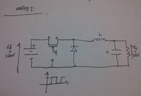
I am designing a 100V-28V DC-DC Buck converter but has encountered a problem when choosing a suitable high-frequency switch. As suggested by many designers online, pMOS is preferred for Buck operation. However one big issue is the limitation of the Vgs (typ: +-20V) which I believe is the reason why I could not utilize this as what other designers usually do.

As seen in the attached schematic, in order to turn off the pMOS switch, Vg must not be lower than both Vs and Vd by the threshold voltage indicated by the manufacturer. That is, |Vgs|< |Vth| & |Vgd| < |Vth|. Since Vs is always 100V (because source is tied to +ve terminal of battery) and Vd = 28V (assuming the capacitor is large enough to hold the charge, hence o/p voltage well) and assuming the Vth is -4V, is it correct that to turn switch off, Vg must be > Vs-|Vth| and also Vg > Vd-|Vth| since a pure MOSFET drain and source is interchangeable.

If this is true, a typical pMOS with only Vgs max of 20V could not handle since we must ramp up Vg all the way to 96V and above (for my case) but that also implies the potential difference between Vg and Vd is 68V which is > 20V and thus the FET will breakdown.

Assuming my source (Vs) and drain voltage (Vd) is always held constant at 100V and 28V respectively, and also assume the pMOS has a threshold voltage of a typical value of -4V. In order to cut off the switch totally, we knew Vg (gate voltage) must be at least > 96V since criteria for MOSFET to operate in the cutoff region is |Vgs| < |Vth|.

And in this particular case, assuming I've set Vg = 100V so that Vgs would be 0 and Vg is so much higher than Vd (about 100-28=72V), therefore both side would not be conducting and hence pMOS operate into the cut-off region. Now, this 72V across the gate and drain is my biggest concern because the manufacturer stated max Vgs = 20V, and since a MOSFET drain and source is interchangeable, therefore I should also assume that the max Vgs also implies the max of Vgd? And if true, shouldn't the Zener diode should protect the potential between gate and drain instead of gate and source?

And if everything I've explained is true, is there a way to overcome this? TIA.
 

since a MOSFET drain and source is interchangeable, therefore I should also assume that the max Vgs also implies the max of Vgd
The assumption is completely wrong for power MOSFET. Maximum Vgd can be calculated by combining Vds and Vgs ratings.

It's not unusual to have input or bus voltage higher than maximum Vgs and in all these cases, the gate driver needs to implement some kind of Vgs voltage limiting. A simple driver would use a PMOSFET as assumed in your circuit, a zener diode resistor circuit between gate and source and a transistor current source to span the voltage difference. If fast gate drive is an objective, a push-pull driver stacked below Vin can be used.

An alternative is a NMOSFET with a standard level shifting high-side driver. But it needs an auxilary circuit to charge the bootstrap capacitor.
 

it would be better to design with N-CH mosfet like irf540 that is robust and very cheap.
P-CH 100v buck design is not a good and up to date solution.
For driving high side n_ch mos just search the IRF.com and you will find excellent drivers.
besides you can go with synchronous buck with two irf540 and one half bridge driver from IR with minimum components.
Check this out:
**broken link removed**
 

The assumption is completely wrong for power MOSFET. Maximum Vgd can be calculated by combining Vds and Vgs ratings.

It's not unusual to have input or bus voltage higher than maximum Vgs and in all these cases, the gate driver needs to implement some kind of Vgs voltage limiting. A simple driver would use a PMOSFET as assumed in your circuit, a zener diode resistor circuit between gate and source and a transistor current source to span the voltage difference. If fast gate drive is an objective, a push-pull driver stacked below Vin can be used.

An alternative is a NMOSFET with a standard level shifting high-side driver. But it needs an auxilary circuit to charge the bootstrap capacitor.

Thanks FvM for your kind assistance.

Since my assumption in determining Vgd max is wrong as above, if I connect this mosfet -> **broken link removed** into my circuit, and swing Vg (reference to common GND) between 90V and 100V, that is operating the pMOS in the linear/ohmic region (when Vg = 90V, hence switch considered turned ON) and cutoff region (when Vg = 100V). Would it work from the theory point-of-view?

And also do you have an example of the "transistor current source to span the voltage difference" schematic? I would like to research more on that area.

Thanks in advance (TIA).

---------- Post added at 14:36 ---------- Previous post was at 12:51 ----------

it would be better to design with N-CH mosfet like irf540 that is robust and very cheap.
P-CH 100v buck design is not a good and up to date solution.
For driving high side n_ch mos just search the IRF.com and you will find excellent drivers.
besides you can go with synchronous buck with two irf540 and one half bridge driver from IR with minimum components.
Check this out:
**broken link removed**

Thank you Mehrshad74 for your reply.

In fact, I've done my own research in using a nMOS.

Based on this application note --> http://www.irf.com/technical-info/appnotes/an-978.pdf and looking at Figure 23 within, the IRD450 highly rated MOSFET seems like an overkill for my design requirements, therefore I would like to know if I could replace that with this nMOS --> http://www.irf.com/product-info/datasheets/data/irl510pbf.pdf.

Also would the IR2117 (http://www.farnell.com/datasheets/59982.pdf) HV floating gate driver IC a better option than IR2183? The high voltage demonstration in its application notes gives me a relief.

Thank you.
 
Last edited:

There are many new 200v N mosfets with very low RDS . IRF540(not 450!) is fine for under 5A application.
IR2183 has more powerful output in comparison with IR2117 and it will be important for driving larger mosfets at higher frequencies.
IR2117 is fine for IGBT driving .
 

As previously mentioned, a bootstrap driver for a single transistor buck converter needs an auxilary circuit to charge the bootstrap capacitor. IR20153 is an example of a driver integrating this feature.
 

There are many new 200v N mosfets with very low RDS . IRF540(not 450!) is fine for under 5A application.
IR2183 has more powerful output in comparison with IR2117 and it will be important for driving larger mosfets at higher frequencies.
IR2117 is fine for IGBT driving .

Hi Mehrshad74,

I've selected the IRL510PBF nMOS (http://www.irf.com/product-info/datasheets/data/irl510pbf.pdf) due to its low Vgs(th) = 2V. Could I use this instead of the suggested IRF450.

I've been selecting MOSFETs based on only the:

i) Vgs(th)
ii) Vgs max
iii) Vds (important since the FET must withstand the huge potential (100V for my case when switch is OFF)
iv) Ids max - which is about 2.5714A as calculated
v) Rds(on) - As low as possible

The rest of the info in the datasheet I've ignored, did I miss anything that I should consider too as it is important?
 

No!
IRL510 is a 100V mosfet and it has large rds. 100v is not safe for a 100v converter.
Vth and Vgs max are not important with IR drivers.
Use a 200v mosfet like IRF640.
 
As previously mentioned, a bootstrap driver for a single transistor buck converter needs an auxilary circuit to charge the bootstrap capacitor. IR20153 is an example of a driver integrating this feature.
But a bootstrapping driver is problematic with single switch buck converters, since the bootstrap capacitor may not necessarily be charged prior to the start of operation. It can be done, but not without careful consideration to circuit startup.

edit: oh nevermind that's what you were referring to. Yes it looks like there are ICs which do this automatically, very nice.
 
Last edited:

But a bootstrapping driver is problematic with single switch buck converters, since the bootstrap capacitor may not necessarily be charged prior to the start of operation. It can be done, but not without careful consideration to circuit startup.

To solve this, could I take out the bootstrap capacitor, charge it, and release it back to the circuit? Does this helps in the startup problem you've drawn?
 

To solve this, could I take out the bootstrap capacitor, charge it, and release it back to the circuit?
Yes but doing this safely is difficult, given that the common mode voltage of the bootstrap capacitor will depend on exactly how you power up the circuit, what the load is doing, etc... the simplest way I can see to do it is to actually have a small FET in parallel with the catch diode. Before starting the converter, you turn it on briefly, which will charge the bootstrap cap, and then immediately start running the converter before it discharges. But you'd have to make sure the small startup FET and the main buck converter FET never operate at the same time.

What is your input/output voltage range? This may be an application where a gate drive transformer is the best solution.

Hi mtwieg,

Thanks for your reply. My input voltage spans from 110v max to 70v min, but nominal at 100v. Output fixed at 28v constant no matter what.
 

For solving bootstrap charging you have 2 solution:
1-using mosfet instead of diode.(sync. rectification)
2-using a dummy load
I suggest number one because its more efficient without any need to additional component.
 

Hi mtwieg,

Thanks for your reply. My input voltage spans from 110v max to 70v min, but nominal at 100v. Output fixed at 28v constant no matter what.
A gate drive transformer is probably easiest for you then, assuming it's correctly designed and you're not trying to operate at very high frequencies.
 

Ok guys, I have just realised that my free-wheeling diode may have been chosen incorrectly. Consider my Buck circuit as attached in my maiden post, if O/P voltage is assumed to be 28V, Pout = ~100W and therefore Iout = Pout/Vout = ~3.5714V.

Under ideal case:

Iin X Vin = Iout X Vout, therefore Iin = Vout/Vin X Iout = D X Iout -------- (1) (since D = Vout/Vin). On the other hand we also know that Iout is a summation of Iin and ID (free-wheeling diode DC current) and hence Iout = Iin + ID ---------- (2).

Therefore to choose an appropriate Schottky diode ratings, I've selected one with rated If(av) = 3A, because my ID = Iout - Iin = Iout - (D X Iout) sub eqn (1) => Iin = Iout[1-D] = 3.5714 X 0.72 = 2.5714A and hence why 3A.

Could anyone verify? Thanks.
 

Hi guys,

Assuming I am using the relocation of Rgate and adding a schottky diode between Vs PIN of the IR2117 driver and COM, wouldn't it be redundant since this schottky to be added as recommended in most guide would exactly has the same Vf(max) rating as my neighbor free-wheeling diode since both schottky has to withstand a Vrrm of >100V (ie: 150V diode)? Is the only difference between these 2 diodes is the average current that passing through it?
 

Hi intelligent minds,

I've chosen to substitute the IR2117 with an optocoupler as my gate driver now. Have been in some research and have found out that the HCPNW-3120 is quite suitable for such high freq. operation (100kHz for my case).

Basically 3 main questions to address:


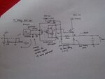
  1. Could I connect the bootstrap circuit (see attached) for the optocoupler using the orginal designed circuitry for the IR2117 as attached in earlier post?
  2. How would the adjacent diode of the free-wheeling as suggested in most bootstrap guides succeeds in preventing the Ve PIN not falling lower than the potential of (GND-Vf of the free-wheeling diode). Based on the fact that both Schottky are the same. Could it be because the free-wheeling diode (on the right) conducts more current than its neighbor diode (on the left) and hence the forward voltage drop of one diode would be higher than the other in nature?
  3. Based on the datasheet of the optocoupler: https://www.farnell.com/datasheets/652282.pdf, should I add a resistor between point A & B (see attached) to 1) limit the input current and 2) lower the voltage drop to the recommended range of 1.5V?

Thanks in advance.
 

Attachments

  • IMG-20111209-00473.jpg
    IMG-20111209-00473.jpg
    1.7 MB · Views: 165

Hi intelligent minds,

I've chosen to substitute the IR2117 with an optocoupler as my gate driver now. Have been in some research and have found out that the HCPNW-3120 is quite suitable for such high freq. operation (100kHz for my case).

Basically 3 main questions to address:


  1. Could I connect the bootstrap circuit (see attached) for the optocoupler using the orginal designed circuitry for the IR2117 as attached in earlier post?
  2. How would the adjacent diode of the free-wheeling as suggested in most bootstrap guides succeeds in preventing the Ve PIN not falling lower than the potential of (GND-Vf of the free-wheeling diode). Based on the fact that both Schottky are the same. Could it be because the free-wheeling diode (on the right) conducts more current than its neighbor diode (on the left) and hence the forward voltage drop of one diode would be higher than the other in nature?
  3. Based on the datasheet of the optocoupler: https://www.farnell.com/datasheets/652282.pdf, should I add a resistor between point A & B (see attached) to 1) limit the input current and 2) lower the voltage drop to the recommended range of 1.5V?

Thanks in advance.

I wonder are my questions that hard to get any replies or is it because of some other reasons...
 

The circuit involves a risk to fail in recharging the bootstrap capacitor in some load and PWM duty cycle situations. The problem has been particularly addresses by mtwieg.

I wonder, where the circuit with gate resistor connected to Ve comes from. I don't see it e.g. in the Avagotech datasheet. I don't feel a need for an additional protection diode.

The optocoupler input current should be set to the specfied value, the maximum ratings have to be kept. In most cases, a current limiting resistor will serve this purpose.

Thanks FvM for your reply.

The reason why I relocate the gate resistor is as described in Section 4.4 of the application note: https://www.fairchildsemi.com/an/AN/AN-6076.pdf.

The explanation for the protection diode at the proposed location is also described in the same section of the attached app note. Basically, if you look at Figure 17, the current path to turn-on the main MOSFET is illustrated in Blue. Hence, the 2 locations for the Rgate would have not much different effect in terms of charging the gate capacitance, hence turning on the main FET, but there is a downside for this approach as the charging path would now include Rgate as part of the charging curcuit and no doubt, it'll slow down the charging time constant by a certain value.

In fact, I might not even add a Rgate because of the small enough peak o/p current from my IR2117 driver.

How do you think?

---------- Post added at 23:57 ---------- Previous post was at 23:16 ----------

There are many new 200v N mosfets with very low RDS . IRF540(not 450!) is fine for under 5A application.
IR2183 has more powerful output in comparison with IR2117 and it will be important for driving larger mosfets at higher frequencies.
IR2117 is fine for IGBT driving .

Hi Mehrshad,

I've just realised that the o/p current for IR2117 is just only 200mA! And that is the point where you said why IR2183 has a powerful o/p, and this o/p is actually referring to the drive current which will in turn affects the turn-on/off time of the mosfet, hence switching speed (via dT=dQ/I).

Do you know if the IR2183 can been utilised as a single channel gate driver (like the IR2117 IC)?

Do I need to connect anything on the O/P of the low side channel?

Thank you.
 

Status
Not open for further replies.

Similar threads

Part and Inventory Search

Welcome to EDABoard.com

Sponsor

Back
Top