Continue to Site

Welcome to EDAboard.com

Welcome to our site! EDAboard.com is an international Electronics Discussion Forum focused on EDA software, circuits, schematics, books, theory, papers, asic, pld, 8051, DSP, Network, RF, Analog Design, PCB, Service Manuals... and a whole lot more! To participate you need to register. Registration is free. Click here to register now.

Off signal for shutdown LDO IC.

Status
Not open for further replies.

ducvilla

Member level 3
Joined
Jul 18, 2011
Messages
59
Helped
31
Reputation
62
Reaction score
29
Trophy points
1,298
Activity points
1,656
Hi! Can somebody help me!
I am newbie on analog ic design. I have a problem with off-signal to shutdown the LDO circuit.
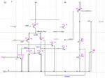
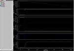
schematic.JPGsimulation_result.JPG
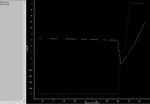
In my circuit, I think when Voff is high, then the transistor XM18 and XM19 is ON, then all other transistors is OFF, then the Vout should be 0V. But when i simulation, all are true except Vout is still high.
Firstly, i think because of charging of capacitor, but it is clear that the charging is only in instance.
Regard.
 

You should actively discharge XM12's gate capacitance to V with another (small) PMOS controlled by OFF_bar (e.g. from XM19's drain).
 

Hi Erikl, Can you explain more detail, because i think when the Vgate of XM12 equal to the Vdd ( it is showed in the simulation), it means that Vg = Vs, then The transistor XM12 will operate in cut-off region, Vout should be 0V. But Vout is still be high ( ~ 1.8V). It not depend on the value of capacitor, because the capacitor effect on the small instance time ( Vout should immediately decrease to 0V)...
Thanks in advanced!
Duc.
 

... then The transistor XM12 will operate in cut-off region ...
True, but this doesn't mean that the charge will disappear immediately. If you simulate for a longer time, you'll see that Vout --> 0 rather slowly. If you want it faster, try the active discharge I mentioned above!
 
Thanks Erikl, you are right, when i simulate in the long duration, Vout reaches to 0V.
I am designing the off-signal for my over temperature protection circuit. In more detail, i make sucessfully the off signal when the temperature is over 140*C, but when the off signal is high, i don't understand why Vout inceases instead of decease to 0V.( i use the same circuit in the first post).

Best regard!
Duc.
 

Sorry, i show the simulation image ( i forgot up this in the previous post):
thermalshut_offsig.JPG

Best regard!
Duc.
 

... i don't understand why Vout inceases instead of decease to 0V.
Also check Pbias, Vref & SIG253 vs. temperature. And then add the "off" PMOS for XM12 !
 

Hi erikl!
The Vpbias, Vref and Vsign253 vs. temperature reaches to the requirement. I simulates with temperature as follow:
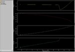
.DC temp -25 160 5. And Vref decrease from 1.21 to 1.17V, Vpbias also changes in the acceptable range to guarantee the current is supplied to each subcircuit. And Vsign253 equals to Vdd when the off-signal is high. You can see these in the simulation:
signal_vs_temperature.JPG
That's why i do not understand why Vout is as simulation.
Thanks Erikl for replying !
 

i do not understand why Vout is as simulation.
Same for me. Are you really sure this isn't deduced from the output cap? Try and repeat the simulation with a reasonable output load!
 
Hi Erikl!
I think my case is not effected by load capacitor, and i simulate without this cap, the result does not change. But i follow your advice, i simulate with output load 6 Ohm, the Vout returns 0V immediately. Can you help me to be more clearly why's that? and why Vout increases in the case no load.

Thanks in advanced!
Duc.
 

Can you help me to be more clearly why's that? and why Vout increases in the case no load.
Hi Duc,
the transistor models take account of bulk & source to drain leakage currents. I guess with your probably huge (6Ω load!) pass transistor XM12, the "off" leakage current isn't negligible, notably if you are simulating in a <≈ 100nm technology. To verify this, try an analysis with a modest DC load, which consumes just a few µA.
Anyway I'd spend an extra disable PMOS for XM12 , as suggested in my answer above.
erikl
 

Hi erikl!
I currently using 600nm process. And i think in this process the leakage current is small. And i have another problem: I think in LDO, all transistors in Error amplifier should be in saturation region, is that right? And Pass transistor should be in saturation or triode region?
Best regard!
Duc.
 

... all transistors in Error amplifier should be in saturation region, is that right?
Yes!

And Pass transistor should be in saturation or triode region?
Depends on its load: for good regulation it should operate in saturation, which is possible for low load currents. For high (max.) load current, however, the pass transistor will unavoidably get into triode region, it's close to dropOut, then.
 
Hi Erikl!
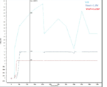
Base on your help, i think my design is ok now. Also i have learned a lots from this. And i realize that my design gets the slow response in order to the following simulation:
simulation_result.png
I think when the Vref reaches to 1.2V, the Vout also obtains 1.8V immediately. But i do not see this in the simulation. Can you explain to me more details about this?

Thank in advanced!
Duc.
 

Seems your Vdd has limited output impedance. Try with a lower time step. But your LDO seems to work fine.
 

Hi Erikl!

Firstly, I want to say thank in advanced for your helps in my problems!
I am appreciate with this!

And to day i have another problems, and i hope you help me be more clear:
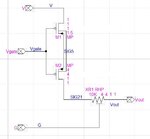
1. In the circuit i attach below: I do not understand its function, and how to drive the Vsource (SIG5) and how is about the Vout?
Q1.JPG
2. And the another one is: with the following circuit, if i only set input is EN, how is about the output? And why the transistor we set gate to source?
Q2_gate_short_to_source.JPG

Thanks!
Duc.
 
  • Like
Reactions: butchi

    butchi

    Points: 2
    Helpful Answer Positive Rating
Status
Not open for further replies.

Part and Inventory Search

Welcome to EDABoard.com

Sponsor

Back
Top