Continue to Site

Welcome to EDAboard.com

Welcome to our site! EDAboard.com is an international Electronics Discussion Forum focused on EDA software, circuits, schematics, books, theory, papers, asic, pld, 8051, DSP, Network, RF, Analog Design, PCB, Service Manuals... and a whole lot more! To participate you need to register. Registration is free. Click here to register now.

How to fill a RAM using VHDL code?

Status
Not open for further replies.

prakashvenugopal

Advanced Member level 1
Joined
Jun 1, 2011
Messages
473
Helped
15
Reputation
30
Reaction score
15
Trophy points
1,298
Activity points
4,973
Hi,

I have to fill a RAM 256x8 using VHDL

ADDRESS : 00 to 256 with Data : 00 to 256

In the Address-->00, the data should be --> 00
In the Address-->01, the data should be --> 01
In the Address-->02, the data should be --> 02
In the Address-->03, the data should be --> 03
"
"
"
"
"
In the Address-->256, the data should be --> 256

Please let me know.

Regards,
V. Prakash
 

A 256x8 RAM has addresses 00 to 255 rather than 256. Initial loading of the RAM content can be easily achieved by a generate statement or an initializing function. If you want to reload the initialization at runtime, you need to provide a sequential process that loads one RAM loacation per clock cycle.
 

Hi,

Did anyone have the sample code for filling the ram 256X8. Please provide me the sample code for it.

thanks,
V. Prakash
 

The problem isn't clear yet:
- internal FPGA block RAM or external RAM, in the latter case, synchronous or asynchronous?
- setting of initial values or reload at runtime?
 

Hi,

1) Internal FPGA BRAM
2) synchronous
3) Reloading at runtime

thanks,
V. Prakash
 

As already mentioned, reloading of the RAM content must be done sequentially, one location pre clock cycle. Something like below:
Code:
signal addr: integer range 0 to 255;
if rising_edge(clk) then
  if do_init = '1' then
    ram(addr) <= std_logic_vector(to_unsigned(addr,8));
    if addr <255 then
      addr <= addr + 1;
    else
      do_init <= '0';
    end if;
  end if;
end if;
 

Hi,

I will check and let you know.

Thanks,
V. Prakash
 

Hi,

I had attached the files for your reference. Please refer.

For every clock rising edge, the data will come from External controller to the FPGA(Din).
For 1st clock - 1st data come from external controller
2nd clock - 2nd data come from external controller
3rd clock - 3rd data come from external controller
----
----
----
255th clock – 255th data come from the external controller

I have to fill this data to the FPGA BRAM, and the same data have to be send to the 8 bit port(Dout) via this BRAM (Dout).

VHDL code for RAM:
*****************************
entity ram is
port (clock : in std_logic;
we : in std_logic;
a : in std_logic_vector(7 downto 0);
di : in std_logic_vector(7 downto 0);
do : out std_logic_vector(7 downto 0));
end ram;

architecture syn of ram is
type ram_type is array (255 downto 0)
of std_logic_vector (7 downto 0);
signal RAM : ram_type;

begin
process (clock)
begin
if (clock'event and clock = '1') then
if (we = '1') then
RAM(conv_integer(a)) <= di;
end if;
end if;
end process;
do <= RAM(conv_integer(a));
end syn;
********************************************

In the above VHDL code for RAM, I had a Address with External Port Entity. I have to use this Address without External Input address from outside. How I can do this in the above code.?

External inputs are clock and Din[7:0] only and Write Enable[we] is pulled up always to write to RAM.The output is Dout[7:0]. How to change this above code as my address is not a external address.? How to do this.

Refer the attachments
Please help me.

Thanks,
V. Prakash
 

Attachments

  • Application_with _ram.doc
    16 KB · Views: 110
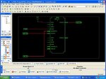
  • RTL_schematic_for_RAM.JPG
    RTL_schematic_for_RAM.JPG
    52.8 KB · Views: 215

External inputs are clock and Din[7:0] only and Write Enable[we] is pulled up always to write to RAM.The output is Dout[7:0]. How to change this above code as my address is not a external address.? How to do this.

The purpose of the code isn't clear. Without addresses, there's not unequivocal relation of data to RAM cells. The same problem apllies to the output data. When do you expect a particular RAM word to be output?

Basically an 8 bit address counter can supply the write address. You'll have to know when to reset or preset it to a particular value.
 
Hi,

1) In case of Ram address--> I will supply a 8 bit counter for 8 bit address of RAM. Same to clock to RAM and 8 bit counter. For Each and every clock, the address will get incremented and the Din data from External controller will change and fill into the corresponding address? am i correct? Please correct me if i am wrong? above code is correct just adding an 8 bit counter to fed the address?

2) In case of output dat --> i have to fill these address 00 to 256 with the Din 8 bit data from external controller and these filled data have to be send to the 8 bit Port (Dout). How to do this? Please let me know

If you are having the RAM code which i was trying, please send that

Please help me.

thanks,
V. Prakash
 

1) The code you have written is just a RAM. How you connect the address is up to you. But your description should work ok.

2) you cannot fill 00 to 256 with the current code, because there are only 256 entries, so the max value will be 255. You will need 9 bits (0 to 511) if you really need to store 256. But your code already reads the output of whatever is stored at the address A, so if you write in a count sequence, the next time you read the RAM you will get the count sequence.
 
Hi,

thanks.

1) Regarding the first point, i will supply a 8 bit counter to the Address bits of RAM with same clock to RAM and 8 bit counter.

2) It is 00 to 255 data only. In the below code, whatever the data which written into the RAM is read immediately. If i have to fill all 255 datas into the address 00 to 255 from external controller and then i have to read and put these datas into the 8 bit Port means, How to change this below code?

After filling the data with 00 to 255, i have to send these data into the 8 bit port. How to do this? Please let me know

First writing 00 to 255 address and then reading the address 00 to 255 to flush into the 8 bit port.

VHDL code for RAM:
*****************************
entity ram is
port (clock : in std_logic;
we : in std_logic;
a : in std_logic_vector(7 downto 0);
di : in std_logic_vector(7 downto 0);
do : out std_logic_vector(7 downto 0));
end ram;

architecture syn of ram is
type ram_type is array (255 downto 0)
of std_logic_vector (7 downto 0);
signal RAM : ram_type;

begin
process (clock)
begin
if (clock'event and clock = '1') then
if (we = '1') then
RAM(conv_integer(a)) <= di; // writing into the ram
end if;
end if;
end process;
do <= RAM(conv_integer(a)); // reading from the ram
end syn;
********************************************


thanks,
V. Prakash
 

Hi Fvm,

Can you please give some idea on this. Please help me in this.

1) Regarding the first point, i will supply a 8 bit counter to the Address bits of RAM with same clock to RAM and 8 bit counter.

2) It is 00 to 255 data only. In the below code, whatever the data which written into the RAM is read immediately. If i have to fill all 255 datas into the address 00 to 255 from external controller and then i have to read and put these datas into the 8 bit Port means, How to change this below code?

After filling the data with 00 to 255, i have to send these data into the 8 bit port. How to do this? Please let me know

First writing 00 to 255 address and then reading the address 00 to 255 to flush into the 8 bit port.

VHDL code for RAM:
*****************************
entity ram is
port (clock : in std_logic;
we : in std_logic;
a : in std_logic_vector(7 downto 0);
di : in std_logic_vector(7 downto 0);
do : out std_logic_vector(7 downto 0));
end ram;

architecture syn of ram is
type ram_type is array (255 downto 0)
of std_logic_vector (7 downto 0);
signal RAM : ram_type;

begin
process (clock)
begin
if (clock'event and clock = '1') then
if (we = '1') then
RAM(conv_integer(a)) <= di; // writing into the ram
end if;
end if;
end process;
do <= RAM(conv_integer(a)); // reading from the ram
end syn;
********************************************


thanks,
V. Prakash
 

There's no specification in the problem about how to write or read. So I would refer to the most simple method. Just add an address counter, that is incremented with every clock cycle. As long as no other specification exists, read and write addresses can be made identical. And I don't see, why read shouldn't be done continuously? Otherwise, there would be a read control signal.
 

I am new for VLSI if you get .Pls forward to me.

I am creating FFT processor for that I need SRAM
 

Hi FVM,

thanks. why read shouldn't be done continuously? Please refer the attachment.

In that, Ram1 = 00 to 255 datas (256 datas) will be sent from the RAM to 8 bit port
In that, Ram2 = 256 to 511 datas (256 datas) will be sent from the RAM to 8 bit port
In that, Ram3 = 512 to 767 datas (256 datas) will be sent from the RAM to 8 bit port
In that, Ram4 = 768 to 1023 datas (256 datas) will be sent from the RAM to 8 bit port
In that, Ram5 = 1024 to 1279 datas (256 datas) will be sent from the RAM to 8 bit port
In that, Ram6 = 1280 to 1535 datas (256 datas) will be sent from the RAM to 8 bit port

Totally i have to send 1536 datas to the 8 bit port in the order of RAM1, RAM2, RAM3,RAM4, RAM5 and RAM6 and again RAM1 data

For this to be done, i have to control the RAM output. Do you have any Sample RAM code with output enable control to control the RAM output to have this in the order of 1,2,3,4,5 and 6.
How to do this.? Please help me.

Thanks,
V. Prakash
 

Attachments

  • Application_Requirement_in_FPGA.doc
    26.5 KB · Views: 117

The so called application requirements are just the "tip of the iceberg", I fear. How long will it take to get a real specification?
 

Hi,

This is the final specification. Before i had send one part of my application with single BRAM. I have to control this 6 RAMS with Output Enable.
in the order of 1,2, 3,4,5 and 6 for 1536 datas. Do you have sample VHDL code for RAM with output enable to control the Individual RAM output. Please let me know. Give an idea.

Thanks,
V. Prakash
 

this is hardly a design spec. It looks more like a back of an envolope drawing.
how are the external data controllers connected to the ram? how are you going to select between rams to put the appropriate one on the 8bit bus to the PC? what has any of this got to do with counters?
 

BRAM has no output enable. Combining the individual RAM outputs can be done by a multiplexer or selector.
 

Status
Not open for further replies.

Part and Inventory Search

Welcome to EDABoard.com

Sponsor

Back
Top