Continue to Site

Welcome to EDAboard.com

Welcome to our site! EDAboard.com is an international Electronics Discussion Forum focused on EDA software, circuits, schematics, books, theory, papers, asic, pld, 8051, DSP, Network, RF, Analog Design, PCB, Service Manuals... and a whole lot more! To participate you need to register. Registration is free. Click here to register now.

MSOP8 clearance errors in Eagle

Status
Not open for further replies.

marki555

Newbie level 3
Joined
Sep 28, 2011
Messages
3
Helped
0
Reputation
0
Reaction score
0
Trophy points
1,281
Location
Slovakia
Activity points
1,311
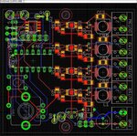
I am designing a board with LED driver LM3407 which comes in eMSOP8 package. I have made the part by modifying standard Eagle library package MSOP8, which has the same pitch of 0.65mm. I have just added the thermal pad. The issue is that DRC shows clearance errors between all pads of that package and I don't know why. I though that it may be due to my NET CLASS for power, but I have removed that - and also the error is for all pads, not only power or connected.
In DRC I had clerance set to 10mil, but I have decreased it to 9mil. The pads are 0.65mm apart and are wide 0.41mm, so should mean the clear space between them should be 0.24mm which is 9.45mil.
Specs of LM3407 is here: **broken link removed**
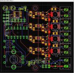
I am attaching my library part of LM3407 and image of the errors on board + the whole board (the routing is ugly, it was first attempt to fix what autoroute wasn't able to route).
shot00158.jpgshot00159.jpgView attachment marki.zip
 

According to the image, the pads copper feature is rather 0.45 mm than 0.41 mm wide.
 
Yes, you are right. I was doing the library 2 months ago and evidently didn't check it throughfully and then just made the calculations using datasheet. I will change the library and will let you know if it helped.
BTW did I make the thermal pad correctly? The dimensions are from the datasheet and I have connected the pad (named EP) to the GND. But the datasheet says also this: "The bottom pad should be connected to ground. For good thermal performance, place 4 to 6 thermal vias from EP to bottom layer PCB ground plane.". What is thermal via? Is it something different than normal via? Because I can't imagine how to put 4-6 vias on such a small place...
 

If you use the Properties button ("i") and show only pads, you can check the size of your pads and change them in your library. Be sure to have your grid set to the proper fineness. Then make a modified package.

John
 

In principle, the exposed pad should have thermal vias. There are different techniques in use, e.g. small open vias, that fill with solder, tented vias, unfortunately reducing the effective pad area or plugged vias with galvanical copper surface.

All these variants are more or less meanings less for a two-layer board as you have. To reduce the thermal resistance, you should connect a sufficient large topside copper area to the pad (without thermal relief, of course).
 
Thanks, I have corrected the package and now I don't have DRC errors anymore. I was also able to make all the routes. Can you please look at the board if you can see something wrong? I plan to put a ground polygon around the LM3407s and the smd parts near it. Should I put a +12v polygon around the diodes and inductors on the right? Can these two be on the same layer?
The board is basically 4x 350mA LED driver with +12V input controlled by PIC16F. The PWM switching frequency is around 150 kHz.
 

Attachments

  • board-12v.jpg
    board-12v.jpg
    274.3 KB · Views: 107
  • board-gnd.jpg
    board-gnd.jpg
    276.5 KB · Views: 101

Status
Not open for further replies.

Part and Inventory Search

Welcome to EDABoard.com

Sponsor

Back
Top