Continue to Site

Welcome to EDAboard.com

Welcome to our site! EDAboard.com is an international Electronics Discussion Forum focused on EDA software, circuits, schematics, books, theory, papers, asic, pld, 8051, DSP, Network, RF, Analog Design, PCB, Service Manuals... and a whole lot more! To participate you need to register. Registration is free. Click here to register now.

Simulation of antenna coil of RFID

Status
Not open for further replies.

shaikss

Full Member level 4
Joined
Jun 18, 2007
Messages
229
Helped
1
Reputation
2
Reaction score
1
Trophy points
1,298
Activity points
3,319
Hi,

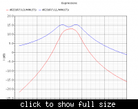
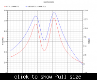
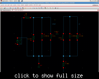
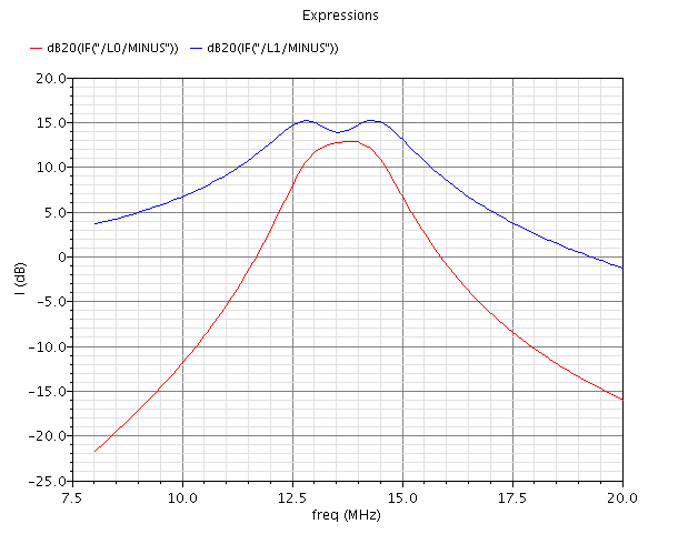
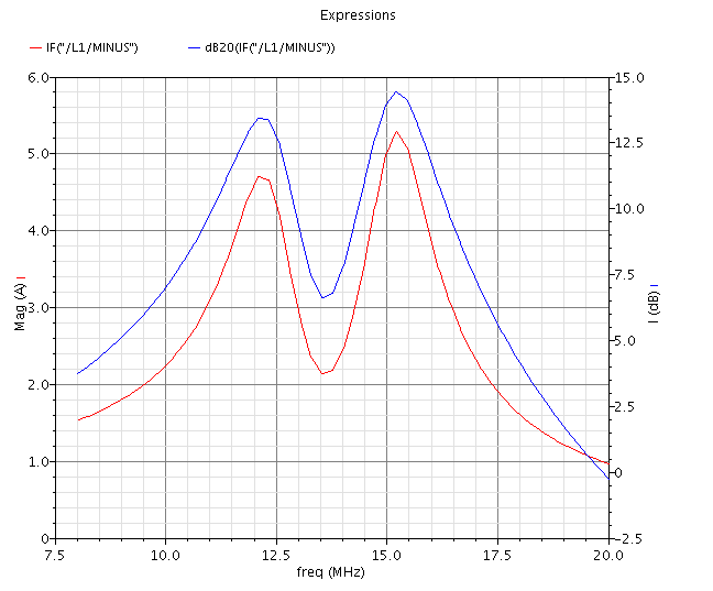
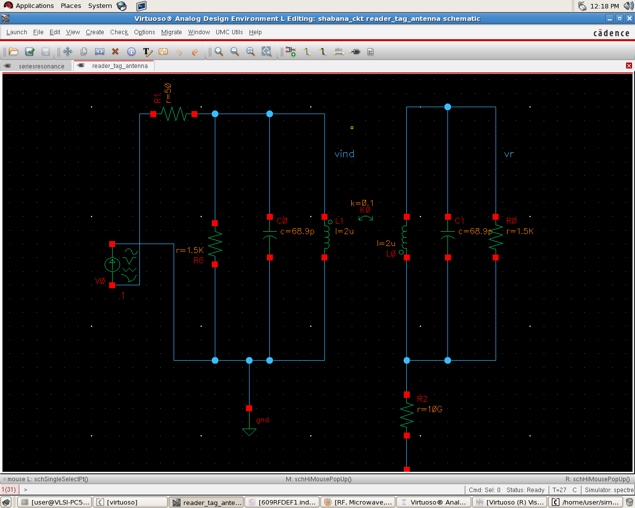
Attached is the schematic and different plots.


The schematic is the antenna coil of the RFID reader and tag. The left part of the schematic (Parallel RLC) is the reader and right is tag.
My Question is: Why is a dip found in the parallel resonant circuit (L1) (Plot of 20dB(L1) Vs frequency?
Why the same dip is not reciprocated into another parallel resonant circuit (L0)after coupling ?
Can you please explain the reason for this behaviour?
By changing the coupling factor, again the dip is varying. How they are dependent?
WHat changes do I need to do in order to see smooth curves?


Thanks,
 

You have a low Q (0.3) reader and a high Q (9) tag circuit. The frequency response shows expectable behavior in this situation. In a visual explanation, the "dip" is caused by the power transfer to the coupled circuit.

But why do want to see smooth curves? What are the design requirements to reader and tag circuit?

In my view, the reader circuit has unsuitable low Q. Usually, the reader Q is set to the maximum value that can be accepted according to bit rate respectively required envelope rise/fall time. Most reader circuits are using a series resonant circuit to achieve the required field strength with low generator voltage.

There are many previous threads discussing different aspects of RFID coil design. Here's a NXP application note, that gives a good introduction

P.S.: I see, that I mentioned the AN already in a previous thread of yours. Referring to the previous discussion of coupling factors, you should consider k=0.1 as a larger value among the expectable range.
 
Last edited:

You have a low Q (0.3) reader and a high Q (9) tag circuit. .

Both reader and tag are parallel resonant circuit. So, Q is 9 at both reader and tag ends.
My doubt is how to design it without getting any dips?

---------- Post added at 10:44 ---------- Previous post was at 10:14 ----------

What are the design requirements to reader and tag circuit?

.


Design Requirements:

1. Designing a sample antenna circuit at HF range.

2. Reader : Freq 13.56MHz, size : Not decided

Tag: Freq : 13.56MHz , Size : 50-cm X 50-cm with a diameter of 15mm
 

Status
Not open for further replies.

Part and Inventory Search

Welcome to EDABoard.com

Sponsor

Back
Top