Continue to Site

Welcome to EDAboard.com

Welcome to our site! EDAboard.com is an international Electronics Discussion Forum focused on EDA software, circuits, schematics, books, theory, papers, asic, pld, 8051, DSP, Network, RF, Analog Design, PCB, Service Manuals... and a whole lot more! To participate you need to register. Registration is free. Click here to register now.

metal widths for the interconnection and routing of the powerMOSes

Status
Not open for further replies.

allennlowaton

Full Member level 5
Joined
Oct 5, 2009
Messages
247
Helped
3
Reputation
6
Reaction score
3
Trophy points
1,298
Location
Taiwan
Activity points
3,061
Hello EDA fellows,
I would like to ask for your help regarding the required or allowable metal widths for the routing of the powerMOSes during
the layout. The devices has 20000um for the widths.
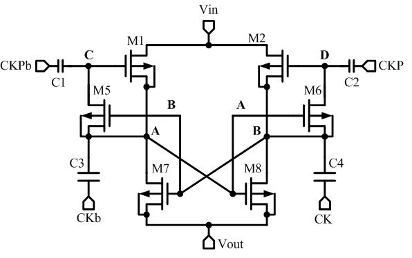
Shown below is the circuit for my charge pump.
The current expected at the output is 80mA.


The current expected at the output is 80mA.

Without knowing your process, here's a rule-of-thumb: Use 1µm/mA [width/current] for commercial/industrial chips (i.e. up to 85°C op.temp.), about twice this value for mil. applications (op.temp. up to 125°C). If possible, you may distribute the resultant width on more than 1 metal layer. Top metal layers often are thicker and so might need just half of such required width.

In sub-micron processes you'll have to take care of slicing wide wires.
 
erikl;953338. If possible said:
this one is not clear to me though. hope you can expound this one for me.
I'm using the 0.35um 5V process
thank you erikl..
 
Last edited:

If possible, you may distribute the resultant width on more than 1 metal layer.
this one is not clear to me

Instead of using 1 metal layer of 80µm width, you could use two 40µm wide metal layers over each other, connected by a via chain. Or 4 metal layers of 20µm widths. If available, use the thick top metal layer.

Then don't use too many vias in between, in order not to block the longitudinal current flow too much.
 
mA/um depends on the layer thickness. You won't go wrong with a 1E5 A/cm2
current density I/(t*w). Beware the via current density, via sidewall can often
be a weak point. Any foundry PDK ought to give you reliability rules of this sort.
 
Typical VIA current density is 1mA/VIA
 

Status
Not open for further replies.

Part and Inventory Search

Welcome to EDABoard.com

Sponsor

Back
Top