shaikss
Full Member level 4
Team,
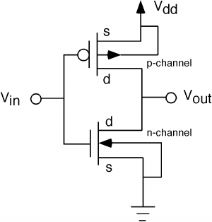
I am terribly shocked and confused after seeing the NMOS and PMOS symbols.
The generic convention for the NMOS and PMOS symbol is the direction of arrow. If the arrow direction is like entering, then the symbol is NMOS and if it is leaving it is PMOS.
Attached 4.48.png is the generic convention. The left image is the generic convention which we all are aware of.
When I tried to design a rectifier using MOS technology, I had taken symbols from analoglib and UMC library. To my great surprise, I found the symbols in different manner.
I have attached the schematic page. It is the right side image. P_18_MM is the PMOS symbol and N_18_MM is the NMOS symbol which are in reverse manner to that of generic. Am I wrong at any point? If so, correct me.
Can you please explain the difference?
Last edited: