Continue to Site

Welcome to EDAboard.com

Welcome to our site! EDAboard.com is an international Electronics Discussion Forum focused on EDA software, circuits, schematics, books, theory, papers, asic, pld, 8051, DSP, Network, RF, Analog Design, PCB, Service Manuals... and a whole lot more! To participate you need to register. Registration is free. Click here to register now.

Netlist difference between LVS layout and schematic in Calibre

Status
Not open for further replies.

nana_7488

Member level 1
Joined
Feb 2, 2010
Messages
32
Helped
0
Reputation
0
Reaction score
0
Trophy points
1,286
Activity points
1,533
Hi all

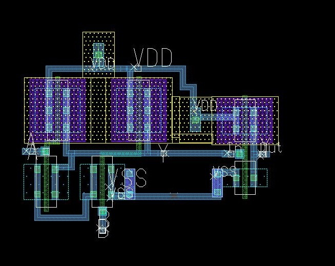
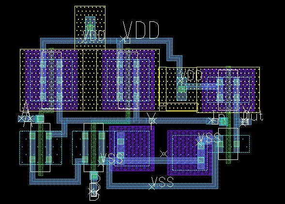
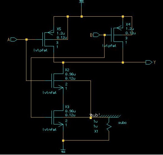
I have a problem with my LVS, it showing missing net in layout and schematic. I've view the netlist between layout and schematic, and it have difference net on the bulk connection of nfet;
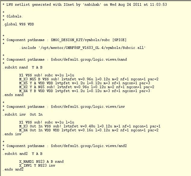
This is my layout netlist
M0 Y A 2 7 lvtnfet w=9.6e-07 l=1.2e-07 m=1 par=1 nf=1 ngcon=1 $X=-2460 $Y=16770 $D=21
M1 VSS B 7 sub! lvtnfet w=9.6e-07 l=1.2e-07 m=1 par=1 nf=1 ngcon=1 $X=-930 $Y=16770 $D=21
M2 Y A VDD VDD lvtpfet w=1.2e-06 l=1.2e-07 m=1 par=1 nf=1 ngcon=1 $X=-2150 $Y=18600 $D=101
M3 Y B VDD VDD lvtpfet w=1.2e-06 l=1.2e-07 m=1 par=1 nf=1 ngcon=1 $X=70 $Y=18600 $D=101

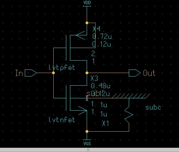
and this is my schematic netlist
M_X3 N$5 B VSS sub! lvtnfet w=0.96u l=0.12u m=2 nf=1 ngcon=1 par=2
M_X5 Y A VDD VDD lvtpfet w=1.2u l=0.12u m=3 nf=1 ngcon=1 par=3
M_X2 Y A N$5 sub! lvtnfet w=0.96u l=0.12u m=2 nf=1 ngcon=1 par=2
M_X4 Y B VDD VDD lvtpfet w=1.2u l=0.12u m=3 nf=1 ngcon=1 par=3

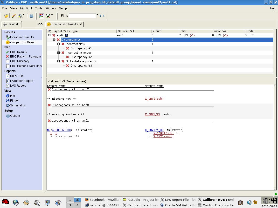
This are my LVS error
LAYOUT NAME SOURCE NAME
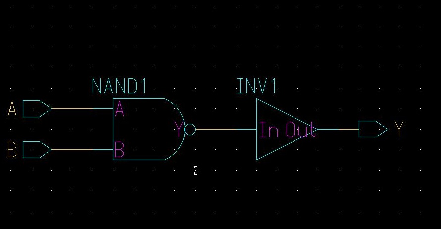
Discrepancy #1 in nand


Net 7 ** no similar net **

Discrepancy #2 in nand


** no similar net ** sub!

For your information, I didnt use subc device in my schematic, but name pull out wire from the bulk as sub!, and I've used ntiedown as substrate contact.

Can anyone tell me why is the netlist difference and how to solve this?I'm really stucked with this...Thanks
 

Re: LVS error in Calibre

...I've used ntiedown as substrate contact

I don't agree with this...ntiedowns are protection diodes NOT substrate contacts.

You must use subc for substrate contacts instantiation in schematic and layout instead!

I have no experience with calibre so if possible try with assura and give me the repsective error report.Also check this thread maybe has the answer to your problem :

https://www.edaboard.com/threads/219922/

What tech do you work on?
 

Re: LVS error in Calibre

ntiedown is not a substrate contact, if you place it on the substrate you will get a diode not a contact
in addition one of your nfets is not connected to N$5 as in the schematic
 

regardless to ntiedown - what is difference in layout between M0 and M1? It looks you shorted drain of M1 to substrate of M0. Do you have substrate P+ connection next to M0 connected to Drain of M1?

Easiest way to look at it would be a picture of your layout.
 

Re: LVS error in Calibre

I don't agree with this...ntiedowns are protection diodes NOT substrate contacts.

You must use subc for substrate contacts instantiation in schematic and layout instead!

I have no experience with calibre so if possible try with assura and give me the repsective error report.Also check this thread maybe has the answer to your problem :

https://www.edaboard.com/threads/219922/

What tech do you work on?

HI Jimito13

Before I've used the ntiedown, I've tried to put subc in my schematic and layout, the LVS clean, but the problem is when I've do the AND gate design using NAND gate and inv that have subc on each design, it give LVS error because I got two subc in top cell (AND gate).

Thanks

I've already tried solution mention in https://www.edaboard.com/threads/219922/, but i dont know how to do inherited connection in calibre. And for your information, i only have calibre to do the DRC and LVS as my Cadence tool already expired. I dont have choices. As I remembered last time I've used Assura with the same design.

---------- Post added at 22:22 ---------- Previous post was at 22:09 ----------

What tech do you work on?

I've used CMRF8SF 130nm IBM tech
 

At first forget tie-downs they are used for other purposes.

Ok,what type of transistors do you use? (regular fets or something else)

Each sub-cell (NAND,Inverter) must have it's own subc at it's schematic and some substrate contacts in it's layout.

The top level AND Gate must have it's own subc at the schematic and some substrate contacts in layout.

All these individual sub contacts of each cell are connected together with metal and finally connected to the VSS (GND or whatever) line of each cell.

Finally you end-up with metal the above sub contacts to the substrate contacts of the top-level and equally to the top level VSS line.

Do the above happen in your layout?

If yes,read the document that i and oermens suggest in the thread https://www.edaboard.com/threads/219922/ and make use of SXCUT.

In my opinion,only in this way you will solve your issue in parallel with IBM's recommendations.

Good luck :)

Hi

I've used symbol of inv and nand gate as top cell of and gate, may I know how I'm going to put subc in the schematic?
I've used lvtnfet and lvtpfet.


Thanks
 

Ok,since the case is the above images and the top-level has no extra devices than need an additional subc,you stay as you are without subc in the top-level.
 

At first forget tie-downs they are used for other purposes.

Ok,what type of transistors do you use? (regular fets or something else)

Each sub-cell (NAND,Inverter) must have it's own subc at it's schematic and some substrate contacts in it's layout.

The top level AND Gate must have it's own subc at the schematic and some substrate contacts in layout.

All these individual sub contacts of each cell are connected together with metal and finally connected to the VSS (GND or whatever) line of each cell.

Finally you end-up with metal the above sub contacts to the substrate contacts of the top-level and equally to the top level VSS line.

Do the above happen in your layout?

If yes,read the document that i and oermens suggest in the thread https://www.edaboard.com/threads/219922/ and make use of SXCUT.

In my opinion,only in this way you will solve your issue in parallel with IBM's recommendations.

Good luck :)

SXCUT:drawing is not used to solve LVS problems but to generate isolated substrate regions, using it for anything else will prevent detection of soft-connect violations
 

SXCUT:drawing is not used to solve LVS problems but to generate isolated substrate regions, using it for anything else will prevent detection of soft-connect violations

I didn't say that SXCUT is used to solve LVS issues.It would be at least foolish the existence of a layer that solves LVS errors (or cheats LVS deck if you want in other words) without having an actual or reasonable purpose in layout.
My intention is to guide nana_7488 to properly use the things that IBM recommends in their documents for proper substrate declaration in layout.
That's all.

Could you please explain the term "soft-connection"?
As fas as i can understand a connection can exist (right or wrong is another matter) or not exist.
 

Hi

I've used symbol of inv and nand gate as top cell of and gate, may I know how I'm going to put subc in the schematic?
I've used lvtnfet and lvtpfet.


Thanks

In your first image I do not see any BP implant, this means you have no substrate contacts in the layout so (assuming this is what you meant to have in the schematic) you just need to stamp the substrate, which you named sub! in the schematic

To name the substrate terminal add a label or pin with the text in SXCUT:label

This layout does not seem to correspond to the initial netlist please post the new netlists if you still have problems

---------- Post added at 10:04 ---------- Previous post was at 10:01 ----------

I didn't say that SXCUT is used to solve LVS issues.It would be at least foolish the existence of a a layer that solves LVS errors (or cheats LVS deck if you want in other words) without having an actual or reasonable purpose in layout.
My intention is to guide nana_7488 to properly use the things that IBM recommends in their documents for proper substrate declaration in layout.
That's all.

Could you please explain the term "soft-connection"?
As fas as i can understand a connection can exist (right or wrong is another matter) or not exist.

soft connections are connections performed through wells (in Calibre language), soft-connect violations are basically shorts in the substrate, differents net names are trying to bias the substrate, using SXCUT:drawing hides these problems and has to be used in very restricted situations not in std digital cells
 

Ok dgnani now it's clear to me the term soft-connections.Thanks for the explanation!
 

In your first image I do not see any BP implant, this means you have no substrate contacts in the layout so (assuming this is what you meant to have in the schematic) you just need to stamp the substrate, which you named sub! in the schematic

To name the substrate terminal add a label or pin with the text in SXCUT:label

This layout does not seem to correspond to the initial netlist please post the new netlists if you still have problems

---------- Post added at 10:04 ---------- Previous post was at 10:01 ----------


Hi dgnani
I have put the subc in the layout for each cell.What do you mean by stamping the substrate and name it?Do I have to name it on layout for inv and nand, or just name it in top layout?
and where should i put the label, is it at the subc? Sorry because I'm too confused between your suggestion and jimito13.

I have try to put global subc in top level schematic, still didn't work, and this layout without the global subc.
please check my layout. Based on your opinion, I can't put SXCUT layer, so do I need it or not?When I tried to put the layer as JImito13 said, other error regarding to subc gone, but as you said, there are soft substrate pin error.


Thanks
 

Your problem is very simple but you keep changing things around and not post all relevant data so...
- pick one configuration
- post the schematic plots of all 3 schematics (top inv and nand)
- post the top-layout
- post both calibre netlists
then we can discuss the solution
 

Your problem is very simple but you keep changing things around and not post all relevant data so...
- pick one configuration
- post the schematic plots of all 3 schematics (top inv and nand)
- post the top-layout
- post both calibre netlists
then we can discuss the solution

Hi.
I don't prefer to put global subc in top shematic

Following are my schematic and netlist


top layout


Hope can solve it because I need to move on to other design.
Thanks
 

please add a "sub!" label to your layout using layer "SXCUT:label" and place it anywhere (outside any device) in your layout...

... and let us know if it works
 
Last edited:
please add a "sub!" label to your layout using layer "SXCUT:label" and place it anywhere (outside any device) in your layout...

... and let us know if it works

Hi

When I add sub! label using SXCUT_NET (as no SXCUT:label in the tech), it happen to have error of missing port sub! in schematic with the 3 error that I've posted before, if I add using SXCUTPIN, the missing port error gone, but the rest of the error still there.
Seem it didn't work.

Any other suggestions?Thanks
 

interesting you must be using a strange flavor of cmrf8sf... anyway the problem seems to be that sub! is not declared as global in the schematic
 

so you suggest I add global sub! in top schematic?
 

I opened an old setup of cmrf8sf that i have (V1.2.1.6 DM) and the layers SXCUT:drw , SXCUT:ll are present...
Did you try to search in LSW the layers from the top menu (option is Set Valid Layers,you will get a long list and search there) ?
 

Status
Not open for further replies.

Part and Inventory Search

Welcome to EDABoard.com

Sponsor

Back
Top