romel_emperado
Advanced Member level 2
- Joined
- Jul 23, 2009
- Messages
- 606
- Helped
- 45
- Reputation
- 132
- Reaction score
- 65
- Trophy points
- 1,318
- Location
- philippines
- Activity points
- 6,061
Re: PIC complete discussion for all
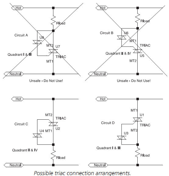
it will work either ways since triac is bidirectional device.. corect me if Im wrong..
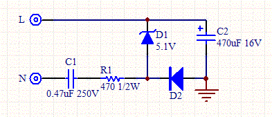
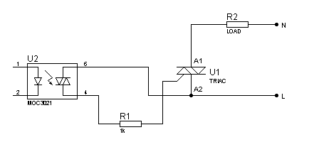
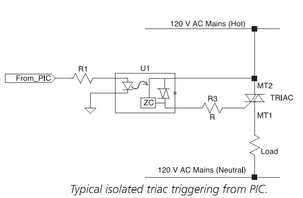
Just a minor remark on the circuit shown on post #5.
The resistor R9 should be connected to pin 1 of the load triac.
That is all
Kerim
")
it will work either ways since triac is bidirectional device.. corect me if Im wrong..