Continue to Site

Welcome to EDAboard.com

Welcome to our site! EDAboard.com is an international Electronics Discussion Forum focused on EDA software, circuits, schematics, books, theory, papers, asic, pld, 8051, DSP, Network, RF, Analog Design, PCB, Service Manuals... and a whole lot more! To participate you need to register. Registration is free. Click here to register now.

why the transient and DC analyses yields different results on Ibias generator circuit

Status
Not open for further replies.
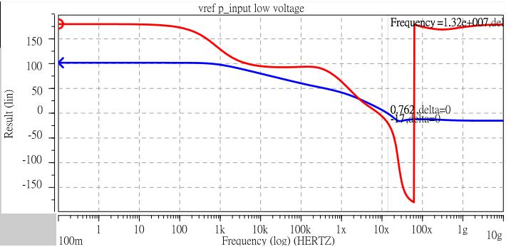
I just used a standard two-stage OP (p-input pairs).

Please, tell us about your "standard two-stage OP".
Did you create your own model? Is it a manufacturer model? Which type?
Which parameters: open-loop gain, input/output impedances?

In particular, the output impedance seems to be "critical". Otherwise I have no explanation for the output voltage that shows NO continuous reduction for rising frequencies (as shown in one of the earlier diagrams).
 
Hi dgnani,

Yes. Compensation component should be necessary even if it is one-stage opamp (fold-cascode can be tried too).
A big cap can be added at the output of OPb. If the dominant pole is low enough and the bandwidth is low enough, the loop could be compensated.


Hi leo

while reducing the number of poles and zeros is definitely the way to go, notice that here the biggest problem here is actually the presence of 2 complex conjugate zeros that create that 'notch' feature in the loop gain, even when we reduce the opamp to a single stage I am not sure that will go away.

I am not sure what creates them (it is basically a gyrated cap somewhere) but adjusting the relative bandwidth of the 3 amplifiers (OPb and the 2 common source amps in the feedback loops) might be key.

One way out of this is too add 2 poles on top of the zeros but it would be nice to understand if there is a more elegant (and practical) way to fix this
 
Please, tell us about your "standard two-stage OP".
Did you create your own model? Is it a manufacturer model? Which type?
Which parameters: open-loop gain, input/output impedances?

In particular, the output impedance seems to be "critical". Otherwise I have no explanation for the output voltage that shows NO continuous reduction for rising frequencies (as shown in one of the earlier diagrams).

I used a real transistors for that OP. The DC gain is around 40dB.
Below are the impedance:
v(vo)/v+ = 86.3035
input resistance at v+ = 1.000e+20
output resistance at v(vo) = 140.5832k
 

I used a real transistors for that OP. The DC gain is around 40dB.
Below are the impedance:
v(vo)/v+ = 86.3035
input resistance at v+ = 1.000e+20
output resistance at v(vo) = 140.5832k

allennlowaton,

I do not understand these data.
Does this mean that your "opamp model" consists of one transistor only? Please clarify.
 
allennlowaton,

I do not understand these data.
Does this mean that your "opamp model" consists of one transistor only? Please clarify.

no no no..a two stage OP using a real transistors..those data were obtained from the .TF(transfer function) command of the HSPICE.
 

Then I repeat my question:
What are the main parametrs of your "opamp" model: gain, input and output resistance?
 
Then I repeat my question:
What are the main parameters of your "opamp" model: gain, input and output resistance?

I don't understand what you mean with that question. I thought you're asking me about the gain ~40dB, input resistance~1e20 and output resistance ~ 140k.
 

OK, now I got it.
You are using an amplifier model with a dc gain of 40 dB and an output resistance of 140 kohms, right?
If this really is the case, I am not surprised about weird simulation results.
The circuitry in your original drawing (posting #1) contains opamps - and I doubt if the models you are going to use can be called "opamp".
At first, you have a gain of only 40 dB (rather than 80...100 dB for classical opamps).
And secondly, a large output resistance of 150 kohms is connected to a gate node of a FET that has an input resistance app. in the same order. In fact, you have a voltage controlled current source, but not an opamp model. I am afraid, that this cannot work as required.

PS: This also explains why the output voltage of your "opamp model" does not decrease down to zero for rising frequencies.
PS2: This also explains the big differences between ideal and "real" amplifier results as reported in posting #5
(ideal: zero output resistance; real: 140 kohms)
 
Last edited:
OK, now I got it.
You are using an amplifier model with a dc gain of 40 dB and an output resistance of 140 kohms, right?
If this really is the case, I am not surprised about weird simulation results.
The circuitry in your original drawing (posting #1) contains opamps - and I doubt if the models you are going to use can be called "opamp".
At first, you have a gain of only 40 dB (rather than 80...100 dB for classical opamps).
And secondly, a large output resistance of 150 kohms is connected to a gate node of a FET that has an input resistance app. in the same order. In fact, you have a voltage controlled current source, but not an opamp model. I am afraid, that this cannot work as required.

PS: This also explains why the output voltage of your "opamp model" does not decrease down to zero for rising frequencies.
PS2: This also explains the big differences between ideal and "real" amplifier results as reported in posting #5
(ideal: zero output resistance; real: 140 kohms)

"a large output resistance of 150 kohms is connected to a gate node of a FET that has an input resistance app. in the same order"??? what kind of FETs are you referring to? in .18um tech gate leakage is completely negligible

While the name opamp is usually reserved for differential amplifiers capable of driving resistive loads, what he is using -an OTA- is perfectly adequate in the current situation where he is driving purely capacitive loads (a little more gain would not hurt but still)

The unusual loop gain behavior at high frequency comes from a large number of zeros (5), which would exist no matter the output impedance of the amplifier

The output resistance of the amplifier only contributes 1 pole to the loop gain, the zeros instead are affected by the gm of the amplifier

In the case of an ideal amplifier some of those zeros are pushed to infinity not by the inifinite resistance but by infinite gm
 
a large output resistance of 150 kohms is connected to a gate node of a FET that has an input resistance app. in the same order"??? what kind of FETs are you referring to? in .18um tech gate leakage is completely negligible

Completely? Independent on frequency? I didn't speak of "leakage" but of the normal load (however, I agree, I should have used the term "impedance" instead of "resistance").

While the name opamp is usually reserved for differential amplifiers capable of driving resistive loads, what he is using -an OTA- is perfectly adequate in the current situation where he is driving purely capacitive loads (a little more gain would not hurt but still)

Does this mean that in the circuit under discussion the opamps (I suppose the used symbols designate voltage output amplifiers) can be replaced by OTA's without influence on the principal function?

If I remember well, it was earlier reported that everything was OK with ideal opamps (with voltage output!).
Or am I wrong?

https://www.edaboard.com/members/256716/
 
Last edited:
I add a 10pF at the OP output and ground.
Below is the result:


The gain at app.~15MHz goes down to zero and stays negative at the higher frequency.
 

Hi allennlowaton,

may I give a general comment? For my opinion, there is to much "trial and error" on your side.
Of course, the "gain" goes down due to a capacitor at the amplifier output (I avoid the term "opamp"), and with 100 pF it will be even lower, but - does this really help?
By the way: In your own interest, be exact to avoid misunderstandings and irrelevant answers. I suppose with "gain" you mean "loop gain", don't you? (Such a circuit has several different "gains"). Are you sure to simulate the loop gain correctly?

To do a systematic approach I recommend the following:
* Where does the whole circuit originate from? Are the shown amplifier symbols in the original circuit opamps or OTA's?
I didn't design such a circuit up to now, therefore my question.
* With "opamp" I mean VCVS . Somebody in the forum is of the opinion an opamp would be a diff. amplifier "capable to drive resistive loads". I think this does not meet the point and is not true (think of active filter applications with capacitive load impedances). To me, an opamp is a high gain amplifier with negligible output resistance. An output resistance of 100 kohms and more belongs - more or less - to a VCCS (OTA with a different symbol as shown!).
* Therefore, try to equip your amplifier model with a low output resistor (at first: ideal buffer) - just to see if this shows good results with a loop gain that crosses the 0 dB line and goes down. And check again the dc bias points.
(As I have asked already in my last posting: Didn't you simulate already with ideal opamps and with success?)
* Then, if the circuit tends to be unstable you/we can think about stabilization methods.
* I am afraid, without some systematic steps you will have no success.

Good luck, regards
LvW

Oh, I forgot to mention another important point:
The methods discussed to simulate the loop gain (L-C method and ac source in series with the amplifier output) are applicable to opamps with low output resistances only!
That means, all loop gain results you have shown up to now exhibit large errors because the load is disconnected from the amplifier output (and the large output resistance).
This is a good example that lack of information (output resistance) leads to severe misinterpretations and false answers. If the output resistance plays a role, the more complicated method to simulate the loop gain as proposed by Middlebrook and others is to be applied.
 
Last edited:
I still think two stage OP should be very difficult to compensate.
Your graph shows several poles that is hard to compensate.
Did you try one-stage OP with cascode output? It will also have enough DC gain. And adding a enough big capacitor at the output of OP, it could be compensated.
I add a 10pF at the OP output and ground.
Below is the result:


The gain at app.~15MHz goes down to zero and stays negative at the higher frequency.
 
Last edited:
a large output resistance of 150 kohms is connected to a gate node of a FET that has an input resistance app. in the same order"??? what kind of FETs are you referring to? in .18um tech gate leakage is completely negligible

Completely? Independent on frequency? I didn't speak of "leakage" but of the normal load (however, I agree, I should have used the term "impedance" instead of "resistance").

While the name opamp is usually reserved for differential amplifiers capable of driving resistive loads, what he is using -an OTA- is perfectly adequate in the current situation where he is driving purely capacitive loads (a little more gain would not hurt but still)

Does this mean that in the circuit under discussion the opamps (I suppose the used symbols designate voltage output amplifiers) can be replaced by OTA's without influence on the principal function?

If I remember well, it was earlier reported that everything was OK with ideal opamps (with voltage output!).
Or am I wrong?

https://www.edaboard.com/members/256716/

Load impedance of the same magnitude as the amplifier output resistance simply means you are looking at a frequency beyond your amplifier bandwidth namely at its -6dB point... this will happen somewhere no matter the output resistance and does not make a difference for this application: it will still work at DC, right?

The only difference between an OTA and an opamp is their output resistance, never seen anybody using a different symbol for it, when you are driving a capacitive load in a DC application you just get a different frequency response

A CMOS amplifier (DC) voltage gain in general will be a product of gm*Rout terms, which indicates gm (or an equivalent gm) is a better design quantity than the voltage gain

an ideal amplifier has infinite gm, which pushes some zeros to infinite frequency, hence the nicer loop gain response; real opamps simply push zeros at higher frequency outside the region of validity of your schematic models, does that really buy you a guaranteed stability?

In any case low output resistance will cost power while compensating an OTA will only cost passive components in the right place

---------- Post added at 11:10 ---------- Previous post was at 10:59 ----------

Hi allennlowaton,

may I give a general comment? For my opinion, there is to much "trial and error" on your side.
Of course, the "gain" goes down due to a capacitor at the amplifier output (I avoid the term "opamp"), and with 100 pF it will be even lower, but - does this really help?
of course it helps, in a system with the same number of poles and zeros you need to fix the behavior at high frequency first, a large cap somewhere has to push it below 0dB
By the way: In your own interest, be exact to avoid misunderstandings and irrelevant answers. I suppose with "gain" you mean "loop gain", don't you? (Such a circuit has several different "gains"). Are you sure to simulate the loop gain correctly?
Man you should be paying attention to your own posts because the loop gain is done (correctly) with an inline probe inserted on the output wire (see your post #47)
To do a systematic approach I recommend the following:
* Where does the whole circuit originate from? Are the shown amplifier symbols in the original circuit opamps or OTA's?
I didn't design such a circuit up to now, therefore my question.
* With "opamp" I mean VCVS . Somebody in the forum is of the opinion an opamp would be a diff. amplifier "capable to drive resistive loads". I think this does not meet the point and is not true (think of active filter applications with capacitive load impedances). To me, an opamp is a high gain amplifier with negligible output resistance. An output resistance of 100 kohms and more belongs - more or less - to a VCCS (OTA with a different symbol as shown!).
interesting: how are a low output resistance amplifier and an amplifier capable of driving resistive loads (w/o losing gain) any different?
* Therefore, try to equip your amplifier model with a low output resistor (at first: ideal buffer) - just to see if this shows good results with a loop gain that crosses the 0 dB line and goes down. And check again the dc bias points.
he already told you he is using real transistors not a model in his simulations
(As I have asked already in my last posting: Didn't you simulate already with ideal opamps and with success?)
* Then, if the circuit tends to be unstable you/we can think about stabilization methods.
* I am afraid, without some systematic steps you will have no success.

Good luck, regards
LvW

Oh, I forgot to mention another important point:
The methods discussed to simulate the loop gain (L-C method and ac source in series with the amplifier output) are applicable to opamps with low output resistances only!
That means, all loop gain results you have shown up to now exhibit large errors because the load is disconnected from the amplifier output (and the large output resistance).
This is a good example that lack of information (output resistance) leads to severe misinterpretations and false answers. If the output resistance plays a role, the more complicated method to simulate the loop gain as proposed by Middlebrook and others is to be applied.

Middlebrook method to measure loop gain uses a single injection probe w/o any input signal nor zeroing, how is this different than what he is already doing?
 
Hi dgnani,

I can't resist to reply again:

Load impedance of the same magnitude as the amplifier output resistance simply means you are looking at a frequency beyond your amplifier bandwidth namely at its -6dB point... this will happen somewhere no matter the output resistance and does not make a difference for this application: it will still work at DC, right?


Up to now I was of the opinion we are discussing stability matters. And you certainly know that an unstable circuit is unstable - independent on the operating frequency. Example: Each student knows (hopefully!) that an uncompensated opamp with 100% feedback is unstable - even if it will be used at dc only.

The only difference between an OTA and an opamp is their output resistance, never seen anybody using a different symbol for it, when you are driving a capacitive load in a DC application you just get a different frequency response

Regarding the OTA symbol: I know a lot of english textbooks dealing with opamps and OTA's. I can't remember a single one that uses the opamp symbol (triangle) for OTA's also.
The following link leads you to one of the earliest and classical publication for OTA applications. I am really surprised that you never have seen the OTA symbol that was used since then in nearly all OTA publications.

**broken link removed**

(In some cases another symbol is used as in the above document: The opamp triangle with a current source symbol at the output node).

of course it helps, in a system with the same number of poles and zeros you need to fix the behavior at high frequency first, a large cap somewhere has to push it below 0dB

In control theory I have learned that this "method" (pure lag compensation) stabilizes a loop "until it is dead".
Of course, you always can reduce the gain until the circuit is stable. But - if the circuit works as required after all?
A very robust method. Therefore my former question: Does it help to solve the problem?

Middlebrook method to measure loop gain uses a single injection probe w/o any input signal nor zeroing, how is this different than what he is already doing?

I recommend to read about Middlebrooks method again. He uses not a single injection probe, but two injection sources in two simulation runs. For your understanding: The second run with a current source is necessary in order to correct the error that was introduced by the first run with a voltage source.
And what is the cause of this error? The finite output resistance of the amplifier! Therfore, for opamp (VCVS) applications one can save this second run; for amplifier with higher output resistances it is an absolute "must".

Thank you
LvW


A final word to allannlowaton:
I hope you are not confused about this discussion. I still recommend to follow all the steps as contained in my posting #72.
 
Last edited:
Hi dgnani,

I can't resist to reply again:
Same here, hopefully we'll all learn something out of this ;)
Load impedance of the same magnitude as the amplifier output resistance simply means you are looking at a frequency beyond your amplifier bandwidth namely at its -6dB point... this will happen somewhere no matter the output resistance and does not make a difference for this application: it will still work at DC, right?


Up to now I was of the opinion we are discussing stability matters. And you certainly know that an unstable circuit is unstable - independent on the operating frequency. Example: Each student knows (hopefully!) that an uncompensated opamp with 100% feedback is unstable - even if it will be used at dc only.
this is why we use compensation
The only difference between an OTA and an opamp is their output resistance, never seen anybody using a different symbol for it, when you are driving a capacitive load in a DC application you just get a different frequency response

Regarding the OTA symbol: I know a lot of english textbooks dealing with opamps and OTA's. I can't remember a single one that uses the opamp symbol (triangle) for OTA's also.
The following link leads you to one of the earliest and classical publication for OTA applications. I am really surprised that you never have seen the OTA symbol that was used since then in nearly all OTA publications.

**broken link removed**
Just by quickly looking on my desk:
Allen, Holberrg 2nd edition; Gray 4th edition; Baker 2nd edition: no use of a separate symbol for OTA, after all most MOS opamp's are indeed OTAs, right?
of course it helps, in a system with the same number of poles and zeros you need to fix the behavior at high frequency first, a large cap somewhere has to push it below 0dB

In control theory I have learned that this "method" (pure lag compensation) stabilizes a loop "until it is dead".
Of course, you always can reduce the gain until the circuit is stable. But - if the circuit works as required after all?
A very robust method. Therefore my former question: Does it help to solve the problem?
what gain reduction? we are simply changing the behavior above the largest pole and zero not the DC gain, which is all we need to operate this circuit (once it is compensated)
by the way this is not the whole compensation just a first step
Middlebrook method to measure loop gain uses a single injection probe w/o any input signal nor zeroing, how is this different than what he is already doing?

I recommend to read about Middlebrooks method again. He uses not a single injection probe, but two injection sources in two simulation runs. For your understanding: The second run with a current source is necessary in order to correct the error that was introduced by the first run with a voltage source.
And what is the cause of this error? The finite output resistance of the amplifier! Therfore, for opamp (VCVS) applications one can save this second run; for amplifier with higher output resistances it is an absolute "must".
we must be reading from different Middlebrooks' **broken link removed**
Thank you
LvW


A final word to allannlowaton:
I hope you are not confused about this discussion. I still recommend to follow all the steps as contained in my posting #72.
 
Last edited:
Good day honorable EDA fellows: dgnani and LvM

I am very much grateful for all your help. I learned an enormous knowledge from both of you.
I will go through all these entries that you've sent and try to absorb all of them.
But for now, the result simulation shown in #54 is quite sufficient already for my application.
Once again, I'm very honored to have you two as my teachers.
 

Quote pancho_hideboo: we must be reading from different Middlebrooks' try this, page 8

I know all the Middlebrook publications, however, for our limited purpose (loop gain only) the GFT manual referenced by you is not the best as it deals with the implementation of the GFT (for other readers: general feedback theorem) into the ICAP simulator. More than that, the GFT can do much more than to simulate the loop gain only.
Nevertheless, of course our problem of loop gain calculation is covered also in this document. But not on page 8, instead
you should read pages 10 pp. Why? Because up to page 10 Middlebrook deals with block diagrams only without interaction (finite input/output impedances). Starting with page 11 (chapter 3) he now considers block interaction as is the case in our circuit under discussion. For clarification, I like to give an excerpt from pages 10,12 (introduction to chapter 3):

Quote Middlebrook (page 10):
The next step is to relate the block diagram of Fig. 3 or 4 to an actual equivalent circuit
model of the system under consideration. This is where difficulties begin to emerge: the conventional
approach attempts to identify the three blocks as containing distinct parts of the circuit, but this is
only true in simple cases. Usually interactions between blocks (loading) impose approximations


page 12:
In the previous section, it was shown how the four second level TFs could in principle be
evaluated by injection of a test signal uz into the block diagram. The difficulties arise when we try
to implement these calculations on the actual circuit diagram instead of on the block diagram. In
particular, is uz a current or a voltage source?
The answer is that, in general, uz is both a current and a voltage source ......


I hope it is clear and obvious now that all amplifiers (assuming uni-directional operation according to Middlebrook) that have a relatively large output resistance require a voltage and a current injection for loop gain calculation.
_______________

dgnani, one last question: In my reply #72 I did nothing else than to help allennlowaton a little by recommending a systematic approach in designing the circuit resp. in finding some error sources. Why do you argue against this ?
I cannot understand.
________________
Regards
LvW
 
Last edited:
Quote pancho_hideboo: we must be reading from different Middlebrooks' try this, page 8
Hi LvW
name calling is probably not ok on this forum (unless of course you are out of supporting arguments)
I know all the Middlebrook publications, however, for our limited purpose (loop gain only) the GFT manual referenced by you is not the best as it deals with the implementation of the GFT (for other readers: general feedback theorem) into the ICAP simulator. More than that, the GFT can do much more than to simulate the loop gain only.
Nevertheless, of course our problem of loop gain calculation is covered also in this document. But not on page 8, instead
you should read pages 10 pp. Why? Because up to page 10 Middlebrook deals with block diagrams only without interaction (finite input/output impedances). Starting with page 11 (chapter 3) he now considers block interaction as is the case in our circuit under discussion. For clarification, I like to give an excerpt from pages 10,12 (introduction to chapter 3):

Quote Middlebrook (page 10):
The next step is to relate the block diagram of Fig. 3 or 4 to an actual equivalent circuit
model of the system under consideration. This is where difficulties begin to emerge: the conventional
approach attempts to identify the three blocks as containing distinct parts of the circuit, but this is
only true in simple cases. Usually interactions between blocks (loading) impose approximations


page 12:
In the previous section, it was shown how the four second level TFs could in principle be
evaluated by injection of a test signal uz into the block diagram. The difficulties arise when we try
to implement these calculations on the actual circuit diagram instead of on the block diagram. In
particular, is uz a current or a voltage source?
The answer is that, in general, uz is both a current and a voltage source ......


I hope it is clear and obvious now that all amplifiers (assuming uni-directional operation according to Middlebrook) that have a relatively large output resistance require a voltage and a current injection for loop gain calculation.
Nope it nor clear not obvious even more so because that paper does not mention anything about what's best for large output resistances and
"The answer is that, in general, uz is both a current and a voltage source"
does not mean that it always has to be, indeed all of the T (loop gain) calculations for GFT can be performed with uz being either a voltage or a current source.
In addition, you can look at page 35 to see how Middlebrook calculates loop gains using single current OR single voltage sources.

All these methods provide a loop gain suitable for studying stability, the advantage of using the GFT method on page 34 is that the result will not depend on where the loop is broken.

In addition the result from using a single voltage source coincide with that general GFT result when the impedance looking backward in the loop is smaller than the impedance looking forward, which is our case at low frequency (since there is no DC conductance looking forward) and become also the case at high frequency once we start loading the amplifier output to move the network towards stability
_______________

dgnani, one last question: In my reply #72 I did nothing else than to help allennlowaton a little by recommending a systematic approach in designing the circuit resp. in finding some error sources. Why do you argue against this ?
I cannot understand.
________________
Regards
LvW

My intent was to avoid teaching someone something inaccurate (like "MOSFET amplifiers driving a capacitive load should have low output impedance"?!), you should also avoid asking (repeatedly) questions that were already answered in previous posts, not to mention the attitude

All in all I appreciate the intent and the interaction, I have have definitely learned a lot thank to this (animated) exchange, I hope you did too
 
Hello, dgnani

At first I like to apologize for allocating a false name to you. I was a bit confused because of another discussion.

I really don't know if it makes much sense to continue the discussion on Middlebrooks methods (plural !) to correctly simulate the loop gain. The GFT manual is a rather complex document (dealing with all kinds of feedback, including bi-directional behaviour) and, thus, not an appropriate source for rather simple circuits.
Nevertheless, I must correct you as far as the following statement is concerned:

Quote dgnani: In addition, you can look at page 35 to see how Middlebrook calculates loop gains using single current OR single voltage sources.

Perhaps you did not recognize that on page 35 Middlebrook speaks about his "third level" transfer functions only.
That means - NOT about the resulting overall loop gain, which consists of several function of different "order" (to be combined to arrive at the final result).
This becomes clear if you read the introduction on page 31:

The General Feedback Theorem (GFT) is a general network theorem that applies to any
transfer function (TF) of a linear system model. The purpose of the GFT is to dissect H, the “first
level” TF of interest, into several “second level” TFs H•, T, Tn, and H0so that insight can be gained
in to how the circuit elements contribute to the result.


In addition - from my simple engineering point of view - it is clear that (in case of a large output resistance) a single series voltage source for injection of a test signal cannot lead to the correct loop gain. For rising frequencies the output voltage of the active device must always goes to zero (right?) - however, the test voltage always creates a voltage drop across the output resistance independent on frequency, thereby inhibiting the zero-going of the output. This error is compensated/corrected by using the second test signal (current). I think this explanation is easy to understand and can clear the point finally.
____________

Finally, if you try to quote me (with quotation marks!) I kindly ask you to do this in a correct way.

Quote dgnani: My intent was to avoid teaching someone something inaccurate (like "MOSFET amplifiers driving a capacitive load should have low output impedance"?!)

Where in my postings did you find the sentence as contained in brackets (with quotation marks)?

Thank you, regards
LvW
 

Status
Not open for further replies.

Part and Inventory Search

Welcome to EDABoard.com

Sponsor

Back
Top