Continue to Site

Welcome to EDAboard.com

Welcome to our site! EDAboard.com is an international Electronics Discussion Forum focused on EDA software, circuits, schematics, books, theory, papers, asic, pld, 8051, DSP, Network, RF, Analog Design, PCB, Service Manuals... and a whole lot more! To participate you need to register. Registration is free. Click here to register now.

why the transient and DC analyses yields different results on Ibias generator circuit

Status
Not open for further replies.

allennlowaton

Full Member level 5
Joined
Oct 5, 2009
Messages
247
Helped
3
Reputation
6
Reaction score
3
Trophy points
1,298
Location
Taiwan
Activity points
3,062
Hello EDA fellows,

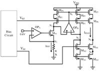
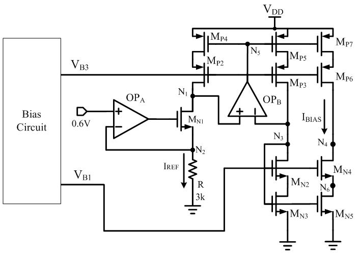
I have been doing this Ibias generator circuit recently.
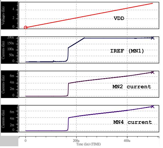
The circuit is shown below.


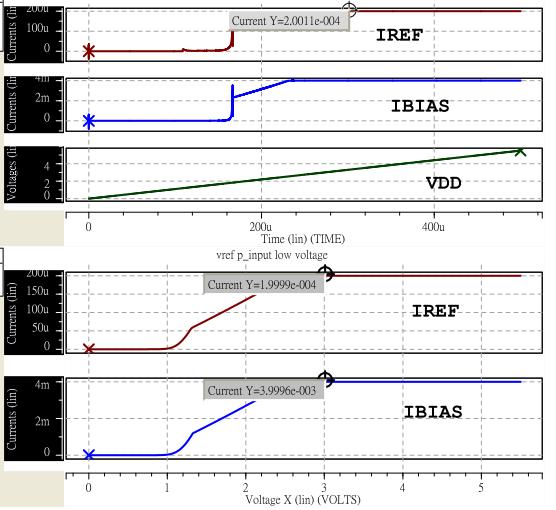
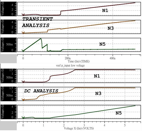
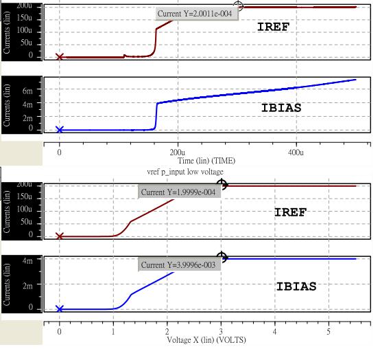
The figure below shows the transient and DC analyses results.

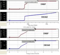
I can't understand why they're not the same.
DC Analysis provides constant current all throughout the desired range
but the transient is increasing. The two simulations share the same simulation paramaters.

Thank you for spending your precious time on this.
 

I suppose, you are simulating with real models for FETs and opamps.
In this case, there must be a difference between between dc and transient behaviour because dc analyses neglect all delays and storage effects within the models (mostly parasitic capacitances).
 
thank you LvW..
Yes, the simulation uses real MOS and OPs.
How can I make the current of the transient to be constant?
 

I made a simulation using an ideal OP for the OPB and the result
is shown below:


My question now is what OP should I'm going to use?
What's wrong with my real OP (a compensated 2-stage)?

---------- Post added at 13:28 ---------- Previous post was at 13:26 ----------

I don't understand this question. What is "the current of the transient" ?

I'm so sorry. What I'm trying to mean is the IBIAS current on the transient analysis. Thank you...
 

I don't think that something is "wrong" with the real opamp model. But it is "real" (in contrast to an ideal model), which means that it has a certain time behaviour. Don't forget that you are simulating in the µsec range.
You should compare your requirements/expectations with the simulation results (on the basis of real models).
Is there a discrepancy yes/not?
 
  • Like
Reactions: allennlowaton

    V

    Points: 2
    Helpful Answer Positive Rating

    allennlowaton

    Points: 2
    Helpful Answer Positive Rating
you shoud try a long time in transient simulation, because the parasitic capancitance may make a long delay while DC analyses ignores parasitic capacitance.
 
From the simulation using the ideal OP, N1 and N3 are at the same potential (1.6V). But the simulation using the real OP shows an N1 and N3 ramping from 2V to 4V. The 2 stage OP had been simulated and it's DC gain is around 70dB with a PM of 70degrees.
I expected that the Ibias current be constant at 4mA from 2.7V to 5.5V input source.

---------- Post added at 15:15 ---------- Previous post was at 15:03 ----------

you shoud try a long time in transient simulation, because the parasitic capancitance may make a long delay while DC analyses ignores parasitic capacitance.

I did a simulation that runs up to 50ms, unfortunately, the output is still the same....
 

hi,

from your description the problem seems to be loss of open-loop gain, this is most likely caused by operating the real opamp outside its input range.

please try simulating the open-loop gain in circuit not standalone, ask if you don't know how
 
Last edited:
allennlowaton, what about the power supply for the opamps? Single oder double?
 
hi,

from your description the problem seems to be loss of open-loop gain, this is most likely caused by operating the real opamp outside its input range.

please try simulating the open-loop gain in circuit not standalone, ask if you don't know how

thank you dgnani...
yes, I don't know where to break the circuit and insert the AC signal as well as the point to be measured. Please teach me.

btw, this is the DC gain and the PM of the 2-stage OP in stand-alone.


---------- Post added at 15:59 ---------- Previous post was at 15:54 ----------

allennlowaton, what about the power supply for the opamps? Single oder double?

The supply, it's single. The Vdd range (2.7V~5.5V) and the ground.
 

It seems to be promising to check if the operational points (dc quiescent output voltages) of both opamps are in the linear region.
I have some doubts.
 
thank you dgnani...
yes, I don't know where to break the circuit and insert the AC signal as well as the point to be measured. Please teach me.
...

hi, the simple way is to break either the opamp positive input wire or the the negative input wire (feedback will carry signal to the other side)
-the formal way would be to break both.

Now use a source with 0V DC amplitude and say 1V of AC amplitude (it does not really matter in this case as you do not use a simplified expression for Aol)

Aol = V(N5) / (V(N1)-V(N3))

V(N1) or V(N3) -whichever you have broken- have to be picked on the opamp side

You can also confirm that the input range is to blame by (do either one of these for a value of VDD where the circuit behaves differently whether using ideal or real opamp):
- changing the standalone AC simulation DC point of the inputs to match the value you get in the bias circuit simulation using the ideal opamp
OR
- by verifying in the DC bias simulation some of the devices (most likely in the input pair) is now working outside saturation region


Now as of this being the only issue, I have doubts because the sim with the real opamp should fail in DC-sweep as well

There might be a second stable OP of the circuit which is privileged by the power-up sequence and creating a startup circuit might be the only way out of this
 
thank you dgnani,
please, correct me if I'm wrong.
I will break either of the positive or negative input of the OP (with the OP still connected with the rest of the circuit).
Insert a 0Vdc and 1Vac and perform AC analysis.
What would be the output node now? Is it the N5 or the N3(that, if I choose the N1 as the input).

For now, I will perform the other test being suggested by you.
 

yes as I mentioned you break either one or both the input wires to the opamp (if you break both just make sure you are creating a net differential signal for the opamp), then use the equation above for Aol
Aol = V(N5) / (V(N1)-V(N3))
since you are looking at open loop gain the output is N5, and the name for the net split by adding the AC source is kept on the opamp side
 
First, I suggest not measuring the last current branch for Ibias. In fact, the circuit can work without MP6, MP7, MnN, MN5. The last branch has two current comparing. The current will not reflect correct current in the second current branch (Mp5).
 
....and the name for the net split by adding the AC source is kept on the opamp side
I didn't understand this and I think that's the reason I'm having a difficulty on plotting the data. I did include these codes the .print vdb(n5) vdb(n3). AOL(dB) = N5(dB) - N3(dB). Is this correct? I inserted the "vn1 vn1 gnd dc 0V ac 1V" at the positive input of the OP.

---------- Post added at 03:15 ---------- Previous post was at 03:04 ----------

First, I suggest not measuring the last current branch for Ibias. In fact, the circuit can work without MP6, MP7, MnN, MN5. The last branch has two current comparing. The current will not reflect correct current in the second current branch (Mp5).

Thank you, leo_o2
The branch of Mp7,6, Mn4,5 provides the 200mV at the node N6 which is badly needed for the next stage. Lower than 200mv would be better in fact.
Shown below are the currents through Mn1, Mn2 and Mn4 during the transient analysis.


---------- Post added at 03:41 ---------- Previous post was at 03:15 ----------

yes as I mentioned you break either one or both the input wires to the opamp (if you break both just make sure you are creating a net differential signal for the opamp), then use the equation above for Aol
Aol = V(N5) / (V(N1)-V(N3))
since you are looking at open loop gain the output is N5, and the name for the net split by adding the AC source is kept on the opamp side

Shown below is the AC analysis result:


My concern now is how to plot the resulted phase. Do I still need to care about it? Thank you..
 

Would you provide waveform for voltage of N1, N3, N5 under both DC and transient with non-ideal OPB?
 
Would you provide waveform for voltage of N1, N3, N5 under both DC and transient with non-ideal OPB?

thank you leo_o2
Shown below are the node voltages waveforms of N1,N3 and N5 both the transient and DC analyses.
 

Thanks. I see. The cascode Mp2, Mp3 should be removed. To keep current of Mp4 equal to that of Mp5, OPb should be used to regulate Mp5's drain and Mp4's drain voltage directly.
In your schematic, there is more than 1 operating point that causes DC is not matched with transient.
 
Status
Not open for further replies.

Part and Inventory Search

Welcome to EDABoard.com

Sponsor

Back
Top