Continue to Site

Welcome to EDAboard.com

Welcome to our site! EDAboard.com is an international Electronics Discussion Forum focused on EDA software, circuits, schematics, books, theory, papers, asic, pld, 8051, DSP, Network, RF, Analog Design, PCB, Service Manuals... and a whole lot more! To participate you need to register. Registration is free. Click here to register now.

Momentary Switch for Power ON/OFF and Input simultaneously (Best practice?)

Status
Not open for further replies.

klausp

Newbie level 4
Joined
Apr 24, 2011
Messages
6
Helped
0
Reputation
0
Reaction score
0
Trophy points
1,281
Activity points
1,348
question.jpg

Hi board,

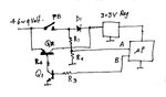
A rough sketch of the circuit is attached.

I'm designing a circuit with the following requirements:

I need switch activated powering of a small microprocessor with a power budget of around 100mA.

Power is activated by holding in the switch for 2 seconds.
Power is deactivated by holding in the switch for 2 seconds.

While power is activated, the switch will function as an input to the microprocessor.

I imagine a starup sequence like this:

1. The switch is pushed in and held in.
2. The processor recieves power through the switch, and starts a timer.
3. When the timer hits 2sec the processor pulls up the PWR pin.
4. The switch is released and the processor now supplies itself through the MOSFET.


While the processor is active, an input should work like this:
1. The switch is pushed and the SWITCH signal goes high.
2. The processor activates a timer.
3. The switch is released before the timer reaches 2sec and the processor knows it was not a poweroff command.


My question is now, am i missing something? Are there any best practices for designing such a circuit?

I have been unable to find a circuit that meets my demands using google.

I plan on using the processor timer for debouncing of the input signal also. Obviously a bouncing during powerup will cause the sequence to restart. I cant see that this should be a problem.

Best regards,
Klaus
 

The Nmosfet can't be used as a high side switch unless you have an isolated power supply to drive the gate (or a bootstrap which can't be applied in your circuit), the cause of the problem is that you need a gate voltage higher than the source pin but when the mosfet conducts you will have a source voltage almost equal to the drain (5v), it that case the gate bias becomes 0v because both gate and source will have the same 5v voltage.

Alex
 
  • Like
Reactions: Tabris

    Tabris

    Points: 2
    Helpful Answer Positive Rating
I designed a similar circuit for a Garage Door Opener circuit.

I used a PNP bipolar transistor to switch the high side and an NPN to switch the base current of the PNP.
 
  • Like
Reactions: Tabris

    Tabris

    Points: 2
    Helpful Answer Positive Rating
Thank you for pointing out my error.

How does one go about activating a low resistance path using only the same voltage level?

i.e using my 3.3v microprocessor output to activate the power?
 

You can solve the mosfet problem using a Pmosfet (source to positive supply and drain as output ) but I have no idea about the rest of your circuit, I haven't done anything similar.

Alex
 

ADP190 can work up to 3.6v (4v absolute max), if you battery has a voltage lower than that (you said 3v3) then you are ok .
The diodes will add a voltage drop so for 100mA and a Schottky diode you can probably expect about 0.5v voltage drop .
You have to check with your mcu if you can apply to the input pin a voltage that is 0.5v higher than the actual power supply because vcc will be through the diode and the input pin will be fed directly from the power supply.

Alex
 

The attached diagram works as follows:-
Press PB, power is applied to the uP via the voltage regulator.
After 3 sec, the uP sets B high.
This turns Q1 on which turns Q2 on thus bypassing PB.
The uP detects when PB is released by polling the voltage on A.

Later, PB is pressed again in order to turn the power off.
The uP detects the high level on A & starts a 3 sec timer.
If A is still high when the timer expires, the uP sets B low & is set into Sleep.

Thus Q1 & Q2 are turned off & when PB is released, the circuit returns to its initial state.

Note:- the programme must be designed to allow for contact bounce from PB.
 

Attachments

  • Pwr sw.jpg
    Pwr sw.jpg
    95.7 KB · Views: 122
Last edited:

Last edited:

My circuit now looks like this:
question3.jpg
VCC is the power for my uP
SWITCH is an input for my uP
PWR is an output of my uP

STARTUP:
The device is started by holding in the switch S1. This powers the uP through D3. With a 3.3v CR2032 battery, the voltage at VCC will be around 3.3v - 0.7v = 2.6v. The uP (CC2540) is rated downto 2v, so i should be ok.
The uP now counts to 2 seconds and pulls up the PWR pin and activates the ADP190 wich send the 3.3v (minus a small voltage loss) through to VCC. The uP has now supplies itself with power.

INPUT:
Pushing the S1 switch pulls up the SWITCH input. No current should go through the diode since the voltage drop across it should be very small when ADP190 is active.
 

Assuming that what you are using is https://www.ti.com/litv/pdf/swrs084 then the datasheet specifies that the voltage in any pin can't be more than 0.3v higher than the VCC supply.
If you provide the input from the button which is connected directly to the battery (3v3) and Vcc is through the diode then you may damage the chip because the input will be over 0.5v compared to the VCC.
You should lower the input voltage with a resistor divider.
Also use Schottky diodes for lower voltage drop.

Alex
 

question4.jpg

Thank you for pointing out my mistake. I have redesigned the circuit and attached it.

With a voltage drop of around 0.3v through the schottky the VCC will be 3v during startup. The
SWITCH input will also be 3v due to the voltage divider.

When the uP is powered through the ADP190, the VCC voltage will be almost 3.3v, and therefore a push on the button should not result in any current running through the schottky.

So far i have avoided a couple of errors due to the help in this thread, and it is greatly appreciated.

If there are anymore suggestions or comments, don't hesitate.
 
Last edited:

Assuming that what you are using is https://www.ti.com/litv/pdf/swrs084 then the datasheet specifies that the voltage in any pin can't be more than 0.3v higher than the VCC supply.
If you provide the input from the button which is connected directly to the battery (3v3) and Vcc is through the diode then you may damage the chip because the input will be over 0.5v compared to the VCC.
You should lower the input voltage with a resistor divider.
Also use Schottky diodes for lower voltage drop.

Alex
You could solve this by connecting a resistor of say 10k between R4/D3 & the Sw input to the uP. Note that this comment refers to your previous circuit.

---------- Post added at 23:14 ---------- Previous post was at 23:08 ----------

View attachment 55687

Thank you for pointing out my mistake. I have redesigned the circuit and attached it.

With a voltage drop of around 0.3v through the schottky the VCC will be 3v during startup. The
SWITCH input will also be 3v due to the voltage divider.

When the uP is powered through the ADP190, the VCC voltage will be almost 3.3v, and therefore a push on the button should not result in any current running through the schottky.

So far i have avoided a couple of errors due to the help in this thread, and it is greatly appreciated.

If there are anymore suggestions or comments, don't hesitate.

The following refers to your latest circuit:- The R5 resistor could be on the uP side as I suggested above. Over voltage on the uP input does not matter, provided that it is current limited.

Your battery is reversed. You have the + plate connected to Gnd.

You appear to be ignoring my circuit. It is a variant of what I did in my garage door opener. I had a 12 Volt supply & needed a 5 Volt regulator for the uP.

It could be adapted to do the function done by the IC in your circuit.
2 transistors & 3 resistors would be cheaper than an IC. Your configuration is good as it does not need the regulator that I included - I needed a reg as I said above.

Also, I suggest that you check the reverse current of the diode D7. The resistor R4 (and in your case, the sum of R4 + R5) must be low enough to prevent the reverse current raising the voltage at SW to a point where it will be recognised as a high by the uP.

Also, have you checked whether the IC will work at 3 Volt?
MOS devices need adequate Gate to Source voltage to turn them on, so a 3 V supply may not be enough.
 
Last edited:

What you need is a design that doesnt consume any current when off. If your hardware is not processor based, get a cmos t flip flop, keying the t input while the output drives a n or p channel mosfet depending on the power pin you want to switch

---------- Post added at 00:44 ---------- Previous post was at 00:37 ----------

What you need is a design that doesnt consume any current when off. If your hardware is not processor based, get a cmos t flip flop, keying the t input while the output drives a n or p channel mosfet depending on the power pin you want to switch

---------- Post added at 00:44 ---------- Previous post was at 00:44 ----------

What you need is a design that doesnt consume any current when off. If your hardware is not processor based, get a cmos t flip flop, keying the t input while the output drives a n or p channel mosfet depending on the power pin you want to switch

---------- Post added at 00:47 ---------- Previous post was at 00:44 ----------

What you need is a design that doesnt consume any current when off. If your hardware is not processor based, get a cmos t flip flop, keying the t input while the output drives a n or p channel mosfet depending on the power pin you want to switch

---------- Post added at 00:49 ---------- Previous post was at 00:47 ----------

What you need is a design that doesnt consume any current when off. If your hardware is not processor based, get a cmos t flip flop, keying the t input while the output drives a n or p channel mosfet depending on the power pin you want to switch

---------- Post added at 00:51 ---------- Previous post was at 00:49 ----------

What you need is a design that doesnt consume any current when off. If your hardware is not processor based, get a cmos t flip flop, keying the t input while the output drives a n or p channel mosfet depending on the power pin you want to switch

---------- Post added at 00:52 ---------- Previous post was at 00:51 ----------

What you need is a design that doesnt consume any current when off. If your hardware is not processor based, get a cmos t flip flop, keying the t input while the output drives a n or p channel mosfet depending on the power pin you want to switch

---------- Post added at 00:54 ---------- Previous post was at 00:52 ----------

What you need is a design that doesnt consume any current when off. If your hardware is not processor based, get a cmos t flip flop, keying the t input while the output drives a n or p channel mosfet depending on the power pin you want to switch
 

What you need is a design that doesnt consume any current when off. If your hardware is not processor based, get a cmos t flip flop, keying the t input while the output drives a n or p channel mosfet depending on the power pin you want to switch

My suggestion below consumes virtually zero energy when it is off.

The only current is the sum of the Icbo of Q1 & Q2.

For example, the 2N3906 has a max Icbo of 60 nA & the 2N2222 has a max of 10 nA.
 

Attachments

  • Power switch.jpg
    Power switch.jpg
    233.2 KB · Views: 121
Last edited:

What you need is a design that doesnt consume any current when off. If your hardware is not processor based, get a cmos t flip flop, keying the t input while the output drives a n or p channel mosfet depending on the power pin you want to switch

Why did you post the same message 8 times?

Alex
 

ljcox, i like your solution with the two bjt's and i'm going to go with that solution. Especially since it has come to my attention that the Shutdown current (Ioff) of the ADP190 is 1uA. Significantly worse than the 20nA that should be possible with the two 2N2222's.

One of my concerns is batterylife. Since im running of a single CR2032 3v cell, i only have about 220mAh.

The ICBO of 10nA of the 2N2222 gives me a total of 20nA of cutoff current. That is acceptable. However, I would like my design to be pick and placeable and i'm having trouble finding equal or better ICBO in an SMT package. My maximum Vce is 3v and Ice is 150mA.

I will post my redesign later today.

If anyone knows of an equal to the 2N2222 that is pick and placeable i would be very thankfull. My experience is that the ICBO is not a searchable charachteristic of most distributors.


Best regards,
Klaus
 

Status
Not open for further replies.

Part and Inventory Search

Welcome to EDABoard.com

Sponsor

Back
Top