Continue to Site

Welcome to EDAboard.com

Welcome to our site! EDAboard.com is an international Electronics Discussion Forum focused on EDA software, circuits, schematics, books, theory, papers, asic, pld, 8051, DSP, Network, RF, Analog Design, PCB, Service Manuals... and a whole lot more! To participate you need to register. Registration is free. Click here to register now.

TL494 Half Bridge blowing fuse

Status
Not open for further replies.
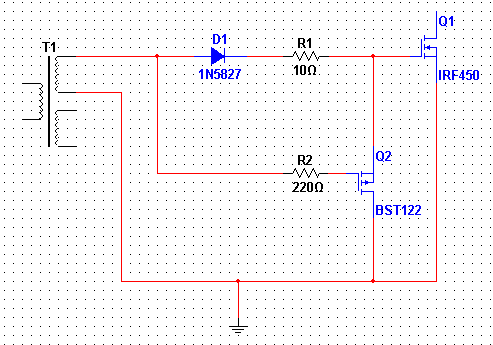
Hi Fvm thanks for the reply. Ok If i consider your first option i.e. Orson's option i would be driving the primary with a push pull CMOS I will search on that. I have some CD4011 handy could that do the job????

Am also thinking is there is any tuning that could be done to the BD139/140 that could help solve this issue?

Regarding your second option, do you have any schematic regarding this.

Thanks
 
Last edited:

CD4000 gates don't have sufficient drive strength, I fear. It won't be an improvement.

For the gate circuit, I don't have a particular idea right now. Some weaknesses of the circuit have been mentioned. If driver IC's are not an option, I would play around with transistors, possibly using to simulator to visualize the effects.
 

Hi FVM thats my exact target right now. I am trying to find a waveform restoration circuit to be added after the GDT secondary to solve the problem. I am also thinking of adding some more deadtime through the TL494 which could help as well. If anybody has a circuit for the gate drive after the GDT secondary to share i would be glad to have a look. thanks
 

There are two things to be suspected .One is the core saturation/magnetization as there is 30secs before blow up at 220VAC .This means the Bmax build up is added on as circuit progresses .The Bmax for the transformer needs to be upgraded to higher ferrite quality .
Another part is that small emitter inductors be provided so that when the top transistors switch off ,only then the ground switch operates.The blowup is principally owing to both transistors switching ON together .The secondary winding is to deplete the charges by a FRR so that cutoff occurs fast ,before the reverse cycle starts .
 

You can try and replace the switch off transistor with a small MOS device.
Top trace is the gate transformer drive, and bottom shows signal on the gate.
56_1305389080.gif

37_1305389606.gif
 
Last edited:

Hi e-design thanks for the circuit i will consider it but do you think it will really solve my issue? I've tried dead time but its of no use, varying the dead time does reduce the signal duty but even at lowest duty that i could set, the step remained in the signal and occupied the signal space instead until i reached 0% duty and everything faded like this: and this is my primary GDT waveform:
68_1305394360.jpg
the source of the problem
 

Hi i've tried to apply deadtime first before doing some tweaking.

1) Does the current waveform start to shape better?

2) for my own learning purposes is this peak in current related to the steps in my waveforms?

Thanks
 

The dead time (assumed) is at the voltage zero crossing ,however , there is delay in current waveform owing to charge storages at the GS capacitance .
This delay causes the mosfet(switch device ) to keep conducting as the reverse voltage is higher ."operates upto 100V but flash break when I go to 220V""It is this Vgs charge not annulled .
I have requested for a n inductance in the drain and gate so that the charges flatten by the arrival of next gate pulse .
 

We'll get to that point later on at least for now the waveforms feeding the mosfet need to be cleaned i don't see the point of doing this now when i have issues with my gate drive waveforms which need to be addressed in first place. Inductance in the gate ok it can add to the process of waveshaping then we can go to the one in the drain. Is there any value you could suggest am sure you are speaking of those iron rings that i've seen in designs after the GDT transfo
 
Last edited:

The gate drive waveforms aren't too bad, they should work - if the zero is as shown. Can you show the circuit you use for the current signal please? I think this may be able to be improved as the waveforms are pretty far from what they should be, also using a CMOS gate to buffer the 494 o/p will work fine - squaring up the edges before going to the transistors drivig the gate drive transformer. Ideally the gate drive transformer should have very low leakage - can you supply construction details so I can check? Regards, Orson Cart.
 

Hi Orson, the current signal is a simple 1 turn primary and approx 100 turns secondary that i harvested out of a pc SMPS. There is no rectification on the secondary and I am using it as a simple means of current monitoring in first place. I will load and rectify the current sense later on for overcurrent protection.

Regarding buffering the 494 output with a CMOS buffer is there any part number you could supply? 74 or 75LS series?

The gate transformer is an EEL16 core , 1:1 turns ratio with 100 turns primary and 100 turns on each secondary. It was built using the Al and reverse calculating for a target inductance of 2mH which gave 100 turns.
 

A current transformer would need a low impedance secondary load, e.g. a 50 ohms oscilloscope input, for unsatured operation and good frequency respectively pulse response. What's your load?
 

Actually i plainly connected it to the oscilloscope probe and its bad.I have gone through how it should be loaded before and after recitifer for desired I and so on but Lets get back to my waveform steps please, it smy major worry right now. Thanks
 

New Vgs
0_1305647694.jpg
.....very basic fix. Will the step on top of the waveform cause any further issues? Am thinking of using a zener to flatten the top. Thanks
 
Last edited:

Will the step on top of the waveform cause any further issues?
No, 10V is sufficient. As explained, the step is caused my the sign reversal of magnetizing current in combination withthze primary driver voltage drop. But no problem so far. What's the circuit modification?

The capacitance of zener diode would slow down the edges, which is unwanted.
 

Hi FVM well i went back to my initial secondary driver scheme. Its a long story but i had dropped it after a fuse and mosfet blow up, after some exchanges here thinking the scheme was bad and went for the simple mosfet + turn off transistor. Anyway thats a thing of the past, here is the gate drive on 5V/Div instead of 10V/Div . I've checked wave timing with respect to ic signal its perfectly in time now. All connections are point soldered now for mosfet drive. I will solder it properly and start investigating the behaviour of the main core and we can start talking about current waveforms going through the main core in case everybody is happy with the current gate waveform.
 

i went back to my initial secondary driver scheme
I see. It's in fact avoiding two diasadvantages of the later circuit, that have been already mentioned.
 

Hi FVM thanks for the reply. Teh initial secondary drive scheme can be found somewhere in this thread. Now that its fixed we can move along
 

Status
Not open for further replies.

Part and Inventory Search

Welcome to EDABoard.com

Sponsor

Back
Top