Continue to Site

Welcome to EDAboard.com

Welcome to our site! EDAboard.com is an international Electronics Discussion Forum focused on EDA software, circuits, schematics, books, theory, papers, asic, pld, 8051, DSP, Network, RF, Analog Design, PCB, Service Manuals... and a whole lot more! To participate you need to register. Registration is free. Click here to register now.

charge pump non overlapping clocks

Status
Not open for further replies.

khaled2k

Member level 2
Joined
May 14, 2009
Messages
51
Helped
3
Reputation
6
Reaction score
3
Trophy points
1,288
Location
Germany
Activity points
1,635
Dear fellows,

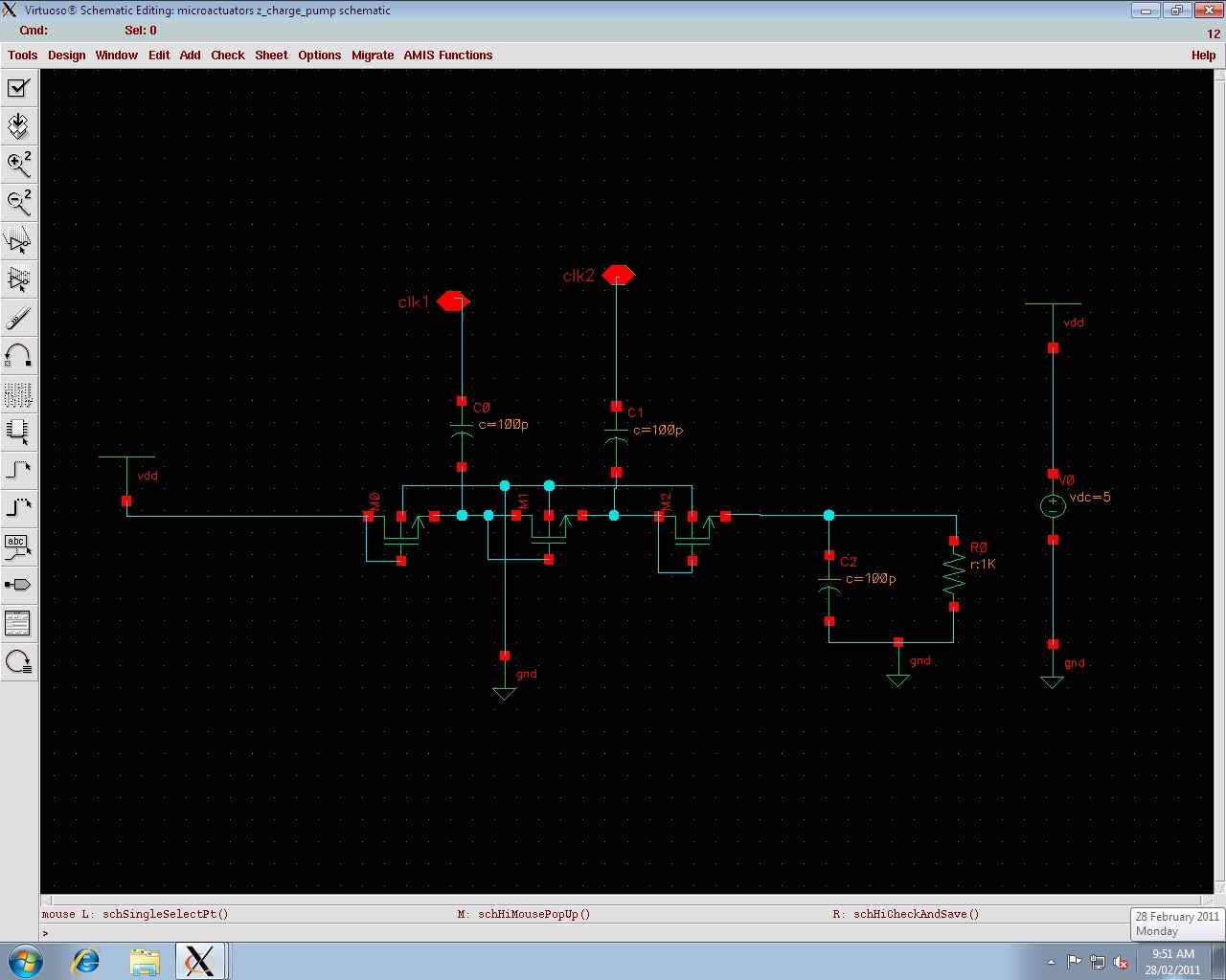
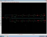
I am designing a CMOS Dickson charge pump. The charge pump works fine when using ideal non-overlapping clock sources (vdc from analogLib).
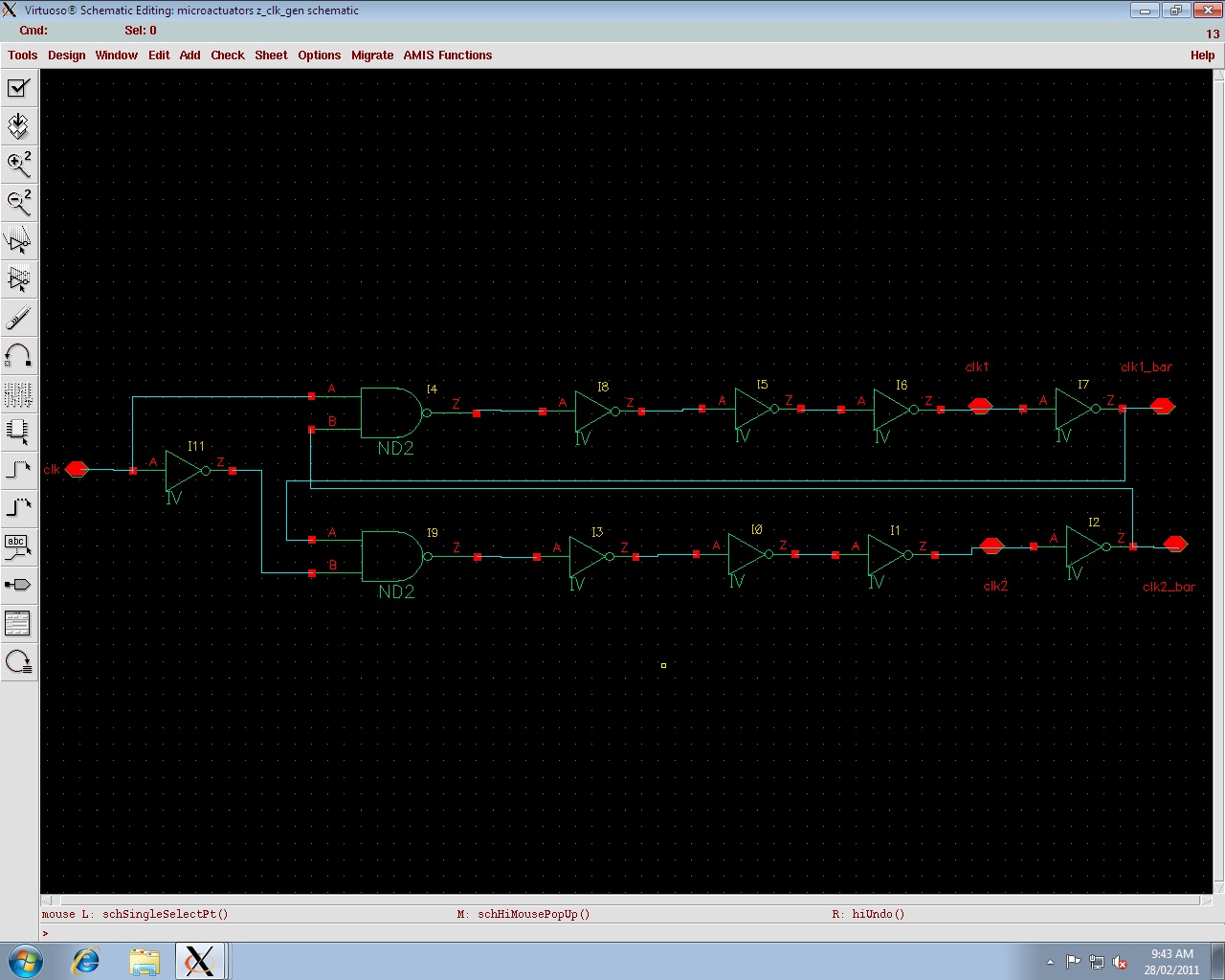
The problem arises when using a clock oscillator (or even an ideal source) and apply it to a circuit to generate the 2 non-overlapping clocks.
When testing the clock generation circuit alone, it generates the clocks fine.
The charge pump with ideal sources is fine too.
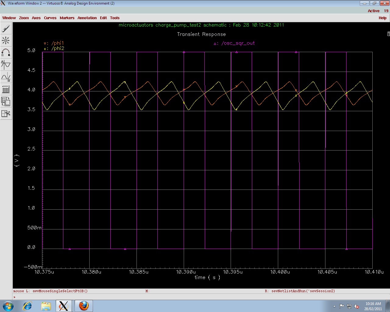
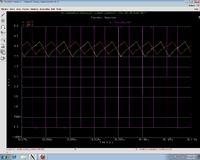
When apply the clock source to clock generation circuit then its output to the charge pump, the clocks (clk1, clk2) output is like shown in figure

I am sure that the clock circuit works fine as a unit and the charge pump as well. The problem when connecting them together.

Thanks in advance


Try loading the CLK1 and CLK2 with the equivalent input capacitance of the charge pump and simulate it again to check the driveability of your inverter I5 and I6. Compare the waveform with and without load.
 

Try loading the CLK1 and CLK2 with the equivalent input capacitance of the charge pump and simulate it again to check the driveability of your inverter I5 and I6. Compare the waveform with and without load.

Hi str3,

For charge pump design, is the required charge pump time constant larger than than the clock frequency?
When tried to apply the clock circuit to an RC circuit (that might be equivalent to the charge pump), I noticed that in order to preserve the form, I should have a large time constant
do you have any idea?
 

The case now is as follows,
using lower frequency, the circuit works fine with a clk source and a circuit converts it to 2 non-overlapping
with high frequency and using TWO vpulse sources, it is fine also
using one clk source and a circuit converts it to 2 non-overlapping at high frequency, the circuit is not working
can anyone advise?
 

maybe the inverter can't properly drive the capacitances at high frequencies?
 

maybe the inverter can't properly drive the capacitances at high frequencies?

Hi Braski,
Thx for your reply.
I use a nominal inverter (0.7um tech) and I use nmos 1/1 and pmos 2.7/1.1
Do you think i should use other dimensions?
 

The maximum frequency your logic gates(ex. inverter) can handle depends on their driveability which is their ability to source (charge) or sink (discharge) the capacitive load. I*t=C*V where I is the source /sink current, t is the time to reach the voltage V from 0v, and C is the capacitive load. For higher frequency of operation, assuming the C and V is constant, you need to increase the I(current). To do that, you may want to increase the sizes of your transistors. Maybe in your library you can find inv1, inv2,inv4 etc...they have the same function but their driveability is different. Inverters in parallel can drive higher capacitances, but beware of the input capacitance as this will also increase, if that is the case, you may also want to increase the drive of the gates before the inverter.
 
The maximum frequency your logic gates(ex. inverter) can handle depends on their driveability which is their ability to source (charge) or sink (discharge) the capacitive load. I*t=C*V where I is the source /sink current, t is the time to reach the voltage V from 0v, and C is the capacitive load. For higher frequency of operation, assuming the C and V is constant, you need to increase the I(current). To do that, you may want to increase the sizes of your transistors. Maybe in your library you can find inv1, inv2,inv4 etc...they have the same function but their driveability is different. Inverters in parallel can drive higher capacitances, but beware of the input capacitance as this will also increase, if that is the case, you may also want to increase the drive of the gates before the inverter.

Thanks str3,

I think this might be the clue of the whole design.
I have inverter cells like inv8 (W/L=30u/0.7u). Can I use higher driving capabilities? for ex. 60u/0.7u or 100u/0.7u? what are the drawbacks for using high W/L?
should I use high W/L also for NAND gates?

Now I have to compromise different things:
- decreasing frequeny, means overall high charge pump resistance which is not suitable for my application
- decreasing pump capacitance means increasing resistance also and output voltage decrease.
I am trying to run simulations to achieve the maximum allowable frequency
 
Last edited:

Thanks str3,

I think this might be the clue of the whole design.
I have inverter cells like inv8 (W/L=30u/0.7u). Can I use higher driving capabilities? for ex. 60u/0.7u or 100u/0.7u? what are the drawbacks for using high W/L?
should I use high W/L also for NAND gates?

you can use higher W/L ratios to better drive the capacitances. the capacitance value of 100 pF is quite high, so it is possible that u may want to use ur custom inverter, instead of cells from the library, properly sizing the ratios (make some calculations about current and charging time to see the frequency).
however, using high W/L in such applications requires that the previous inverter in your non-overlapping generation chain can effectively drive the output inverter transistor gate. In fact, Cin of your inv. will be tied to the CGS of the mos (approximately 2/3*W*L*COX). So, if you work with the minimum L, increasing W will increase the gate area, making more difficult to drive it. However, the Cin of your inverter will be decisively smaller and easier to drive than the 100 pF load, for very big widths. Maybe you can think to add some kind of buffer between clocks line and charge pump, to help the driving.
Another idea is to realize a chain of inverters with progressively increasing widths to avoid the driving problems. But i think this is not the case, i don't think you need a very very high frequency.


later i'll edit this post
 
Last edited:
you can use higher W/L ratios to better drive the capacitances. the capacitance value of 100 pF is quite high, so it is possible that u may want to use ur custom inverter, instead of cells from the library, properly sizing the ratios (make some calculations about current and charging time to see the frequency).
however, using high W/L in such applications requires that the previous inverter in your non-overlapping generation chain can effectively drive the output inverter transistor gate. In fact, Cin of your inv. will be tied to the CGS of the mos (approximately 2/3*W*L). So, if you work with the minimum L, increasing W will increase the gate area, making more difficult to drive it. However, the Cin of your inverter will be decisively smaller and easier to drive than the 100 pF load, for very big widths. Maybe you can think to add some kind of buffer between clocks line and charge pump, to help the driving.
Another idea is to realize a chain of inverters with progressively increasing widths to avoid the driving problems. But i think this is not the case, i don't think you need a very very high frequency.


later i'll edit this post

Thanks Braski, your analysis is neat and clear.

I agree with you regarding the Cgs because if I use 100u/0.7 I will have less than 1pF additional capacitance

So what kind of buffer do you suggest? I mean does it need a digital buffer or a sort of source follower?
I haven't designed a digital buffer before. could you please give me some guidance of specs and design topologies?

regarding progressive W/L inverters, which one should have the largest W/L? is it clock input side or load side?

uhm, i think that 1 pF of Cin could represent some kind of issue if you drive it with a "weak" inverter, depending on the clock frequency, so you have to properly watch all the CIN.

i am not sure about the digital buffer: i think it is simply an inverter cascade to realize a non inverting function with an high driving capability, which is what you need. The specifics regard the frequency you have to achieve, the load capacitance (100 pF). In your case, i don't think there are many others specification. I'm not expert in this field. However, you should have some kind of buffers in your design kit libraries.

The kind of source follower will produce a drop of your voltage level coming from the clock, so i don't think is good (my opinion).

regarding the progressive W/L inverters, they realize a kind of digital buffer: the largest W/L will drive the load capacitance. It is clear: the first inverter is the "weakest", let's say it has 2/1 and 5/1 NMOS and PMOS respectively.. it can easily drive a bit larger inverter, let's say 4/1 and 10/1...this second can easily drive a 8/1 20/1 (the sizing is not real, just to give an example). If you go on, in some steps you will have a "powerful" inverter, able to drive your load, driven by a less powerful, but still adequate to avoid big delays introduced by Cin. However, the chain should be not too long, because every inverter introduces some delay. Try something like that. So, the closer you are to the load, the bigger W/L you should have.

the last thing: make calculation about the charging time of your load to find the correct sizing of the last inverter for your frequency, and then go back to size the previous ones.
 

based on what you wrote - ideal sources - works fine - ideal source gives you infinite drive - therefore the pumps charges correctly.
If you have such a small drivers - you can just take that inverter and load it with cap to gnd. You can see the edge degradation when you increade the load.
I would go first for inverter 100./07 and lets see

Thanks Teddy
I think I am fighting against physics now. To drive 100pF load with 100MHz or 200MHz clock I need an infinite transistor width.
It seems that very large W/L=900u/0.7u is capable to drive 50MHz and 100pF or slightly more.

Is there any way to generate non-overlapping clocks driving such high capacitive loads?

browse the literature, but i think 100 pF to drive at 200 Mhz is very very hard. can't u use smaller loads?
 

browse the literature, but i think 100 pF to drive at 200 Mhz is very very hard. can't u use smaller loads?

The problem that I need high pumping capacitance to produce high output voltage, in other words I need a pumping capacitance much higher than switch (transistor) parasitic capacitance.
 

100 pF is way higher than the parasitics of a small drive. try load of a few pF... a small driver will have parasitics in the order of tens of fF or at max a few hundred of fF. a load of some tens higher would be enough.
 
Status
Not open for further replies.

Part and Inventory Search

Welcome to EDABoard.com

Sponsor

Back
Top