Continue to Site

Welcome to EDAboard.com

Welcome to our site! EDAboard.com is an international Electronics Discussion Forum focused on EDA software, circuits, schematics, books, theory, papers, asic, pld, 8051, DSP, Network, RF, Analog Design, PCB, Service Manuals... and a whole lot more! To participate you need to register. Registration is free. Click here to register now.

high stability LDO with fast transient response

Status
Not open for further replies.

raghuvlsi

Member level 1
Joined
Aug 15, 2007
Messages
35
Helped
0
Reputation
0
Reaction score
0
Trophy points
1,286
Activity points
1,527
hi ,
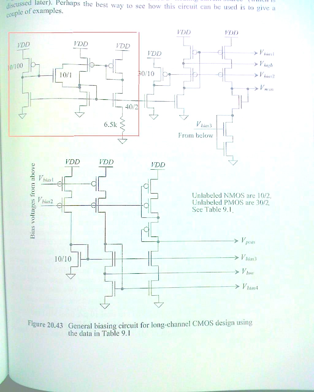
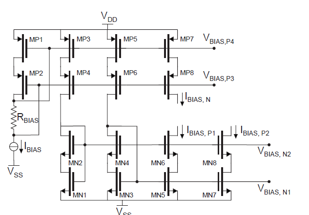
I raghu would like to design voltage regulator with an improved fast transient response.i have attached my base paper.Can any one guide me how to design from base level of voltage regulator and how to design individual blocks initially according to my base paper design with specs of each block.

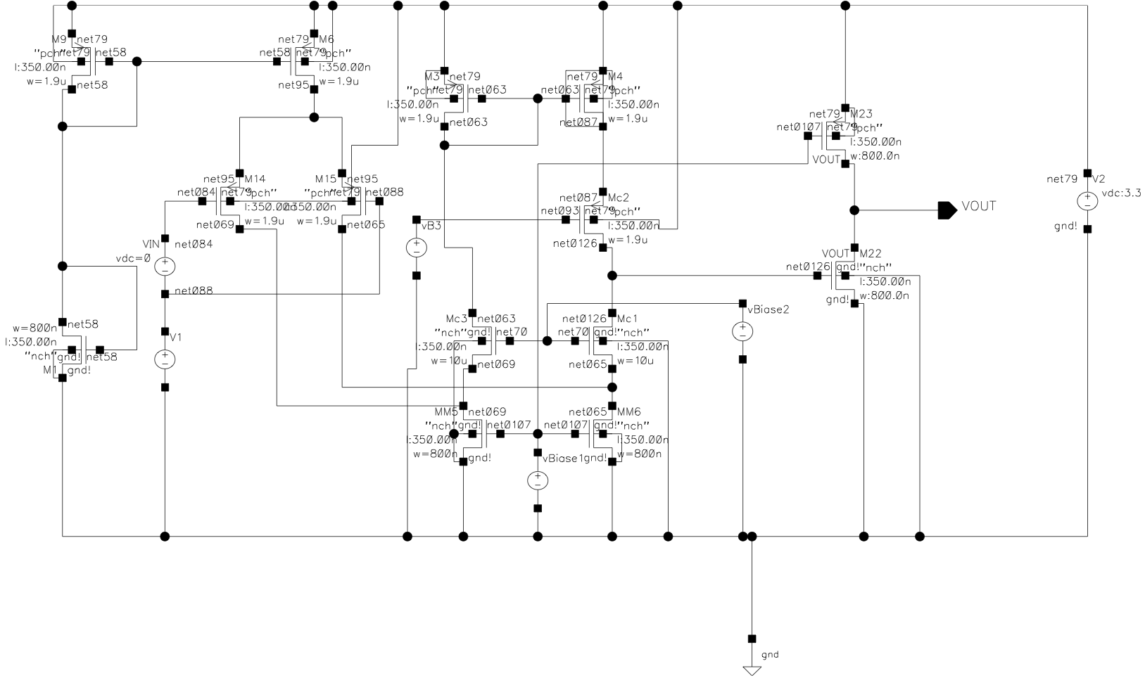
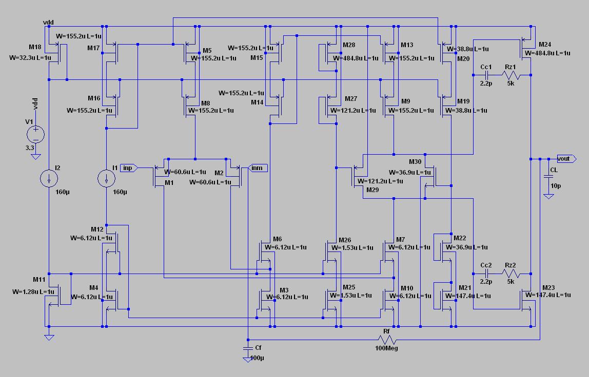
Please tell me what are the specifications i need to take initially based on my base paper design.Right now i planned to design error amplifier which is used "single ended folded cascode OTA" for traditional LDO as mentioned in base paper.

Thanq
 

Attachments

  • BasePaper.pdf
    841.6 KB · Views: 359

Can any one guide me how to design from base level of voltage regulator and how to design individual blocks initially according to my base paper design with specs of each block.

I think your base paper provides a sufficiently good design guidance, even for the single blocks. But you surely can get help here, if you ask specific questions.

Please tell me what are the specifications i need to take initially based on my base paper design.

The specifications of course must be provided by your boss, your prof. or may be by yourself; you might just keep or alter those mentioned in Table 1 (p. 4) of your base paper.

Surely you cannot expect forum members to guess your requirements!
 
Thanks for your reply,
Right now iam designing traditional LDO(fig.1,page number-1) which is mentioned in Base paper.
Error amplifier block(fig.3,page number-2) is using in traditional LDO.
Technology:0.35um.
1)For my design analysis approximately how much 'L' value is required for each transistor to target specifications.I used L=0.35um, but the result is not proper.
2)Band width is how much?
Thanq
 

Hi,
Please tell me the values of
For NMOS->Un,Cox
For PMOS->Up,Cox
Using 0.35um TSMC for my project
Thanq
 

Technology:0.35um.
1)For my design analysis approximately how much 'L' value is required for each transistor to target specifications.I used L=0.35um, but the result is not proper.
Here is a 0.35µm folded cascode OTA design, which uses L=0.35µm throughout. I found it some time ago here on the EDAboard forum, but don't remember where & when, nor do I know if it really worked well:


Here's a 0.35µm HiFreq OpAmp which uses L=1µm for all MOSFET's. I think for good & accurate analog designs it is better to use the 3..4-fold min. length:

As you don't need the AB end stage, you dismiss M7, M9, M10, M13, M19 .. M24, M29 & M30.

This is a paper on 0.35µm OTA designs for 4 different power/bandwidth combinations. It uses an NFET input stage, however: View attachment Folded_Cascode_OTA_designed_through_gm_over_Id.pdf

A similar design comes here - including the necessary CMFB part: View attachment LP-SC-CMFB-Folded-Cascode-OTA_opt.pdf


2)Band width is how much?
As much as you need: this depends on how fast the LDO must react on interferencies, i.e. on input (supply, PSRR) and output (load) changes.
 
  • Like
Reactions: raghuvlsi

    V

    Points: 2
    Helpful Answer Positive Rating

    raghuvlsi

    Points: 2
    Helpful Answer Positive Rating
Thanks for giving valuable information sir,
 

Hi sir,
Please give example values for AC analysis for input of folded cascode OTA. So that i can analyze to force the values in simulation tool(using Mentor graphics DA_IC tool) for AC analysis.
Please send some examples of circuits with AC,DC and transient analysis including values.
Thanq
 

  • Like
Reactions: raghuvlsi

    V

    Points: 2
    Helpful Answer Positive Rating

    raghuvlsi

    Points: 2
    Helpful Answer Positive Rating
Hi sir,
How to get conclusion of Vgs and Vds values of each MOSFET in my design for calculating width.Please give an idea.
Thanq
 

Hi Raghu,

this depends on your circuit, its supply voltage, and the process which you intend to use. It's impossible to tell you any reasonable values if this info isn't available.

Generally you first must learn how to design circuits. There are a lot of good books available on Analog Circuit Design, pls. find here some examples:

Allen/Holberg "CMOS Analog Circuit Design"
David M. Binkley "Tradeoffs and Optimization in Analog CMOS Design"
Behzad Razavi "Design of Analog CMOS Integrated Circuits"

Study such a book thoroughly and you'll learn how to design circuits and calculate their W/L ratios. After this you will be able to either manually calculate values like Vgs or Vds, or you will analyse these values if you have access to a simulator tool.

Have fun by learning!
erikl
 
Hi sir,once please go through my base paper.My project objective is following base paper only.I can't analyzing values of Vgs and Vds for calculation of each MOSFET's width and length in my design. And also i could't find how much bias voltages need for my design.Please let me know if you can analyze my design.Iam using TSMC 0.35um and Vdd=5v.
Any how i started to study those books which referred by you.
Thanq.
 

Attachments

  • BasePaper.pdf
    841.6 KB · Views: 194

Hi sir, i getting confused with how much input current need for my proposed circuit(figure 5.3).
From base paper i could't find input current value.
Please go through Table 1,here i have settling time value[any relation between slew rate and settling time?]. From this can we calculate input current value?if yes how?
(or) can we target with gain for analyze the input current?If yes, how much gain is sufficient for my design?
Note:Iam following base paper parameters only for my project.
I can analyze Vgs and Vds values.
Thanq..
 

... getting confused with how much input current need for my proposed circuit (figure 5.3).
Can't find figure 5.3 in your base paper, sorry!

From base paper i could't find input current value.
Depends on your required BWcl , s. equs. (19) & (18 ) of your base paper.

Please go through Table 1,here i have settling time value[any relation between slew rate and settling time?].
Of course! Settling time = Δt2 ≈ n * ΔVout,max/slew_rate , where the factor n depends on your required max. (in-)accuracy. Use n=3.5 for 3% or n=4.6 for 1% of inaccuracy. n ≈ -ln(max_inaccuracy). This of course is just a rough estimation, because it's based on exponential decay with a time constant of ΔVout,max/slew_rate .

From this can we calculate input current value?if yes how?
Yes, via the required bandwidth BWcl , again s. the equs. (17) through (20).

(or) can we target with gain for analyze the input current?If yes, how much gain is sufficient for my design?
Like the settling time, the necessary gain depends on your required max. inaccuracy:
gain ≥ 1/max_inaccuracy .

HTH! erikl
 
  • Like
Reactions: raghuvlsi

    V

    Points: 2
    Helpful Answer Positive Rating

    raghuvlsi

    Points: 2
    Helpful Answer Positive Rating
thanks for giving valuable information sir,
actually its figure 3 from base paper.I was wrongly typed .
Can we regulate 2.5v with input voltage 4v?reference voltage has mentioned 2.5v
My base paper mentioned 4v to 6v input voltage.
 

Can we regulate 2.5v with input voltage 4v?reference voltage has mentioned 2.5v

This of course depends on the process to be used: if it gives you transistors which can stand the 4V.

An output regulation of 2.5V with input of 4V is easily to be achieved. Usually LDOs are designed for a dropout voltage of a few hundred milliVolts only (at low output currents, say < ≈50mA).
 
Hi sir,
In my base paper (Fig3) i need to generate 2.5v Reference voltage and bias voltages Vb1,Vb2,Vb3,Vb4 and Vb5. Shall i use DC voltage source with corresponding values or i need to generate the circuits?
Do you have any idea about how to analyze bias voltages for particular value.
Thanq
 

... Shall i use DC voltage source with corresponding values or i need to generate the circuits?
This depends on what you want to do with your circuit. In the very beginning of designing your circuit you may work with DC bias voltage or current sources - at least until your main circuit works correctly. But if you intend to produce a real circuit, or even if you want to know how your circuit behaves at different temperatures (and how process variations will change its behaviour), the creation of transistor bias circuits is a MUST.

Do you have any idea about how to analyze bias voltages for particular value.
Analysis is done by simulation. How to design bias circuits is described in any book about Analog Circuit Design.
Below pls. see 2 bias circuit examples (topologies):
 

Hi sir,
Please tell me the values of
For NMOS->Un,Cox
For PMOS->Up,Cox
Using 0.25um TSMC for my project.
Thanq
 

Sorry, I neither have the 0.25um TSMC Design Kit nor its models. You should get these values from their PDK. Until then you could start with the values published with the correspondent MOSIS WAFER ACCEPTANCE TESTS.
 
Status
Not open for further replies.

Part and Inventory Search

Welcome to EDABoard.com

Sponsor

Back
Top