pnjbtr
Full Member level 5
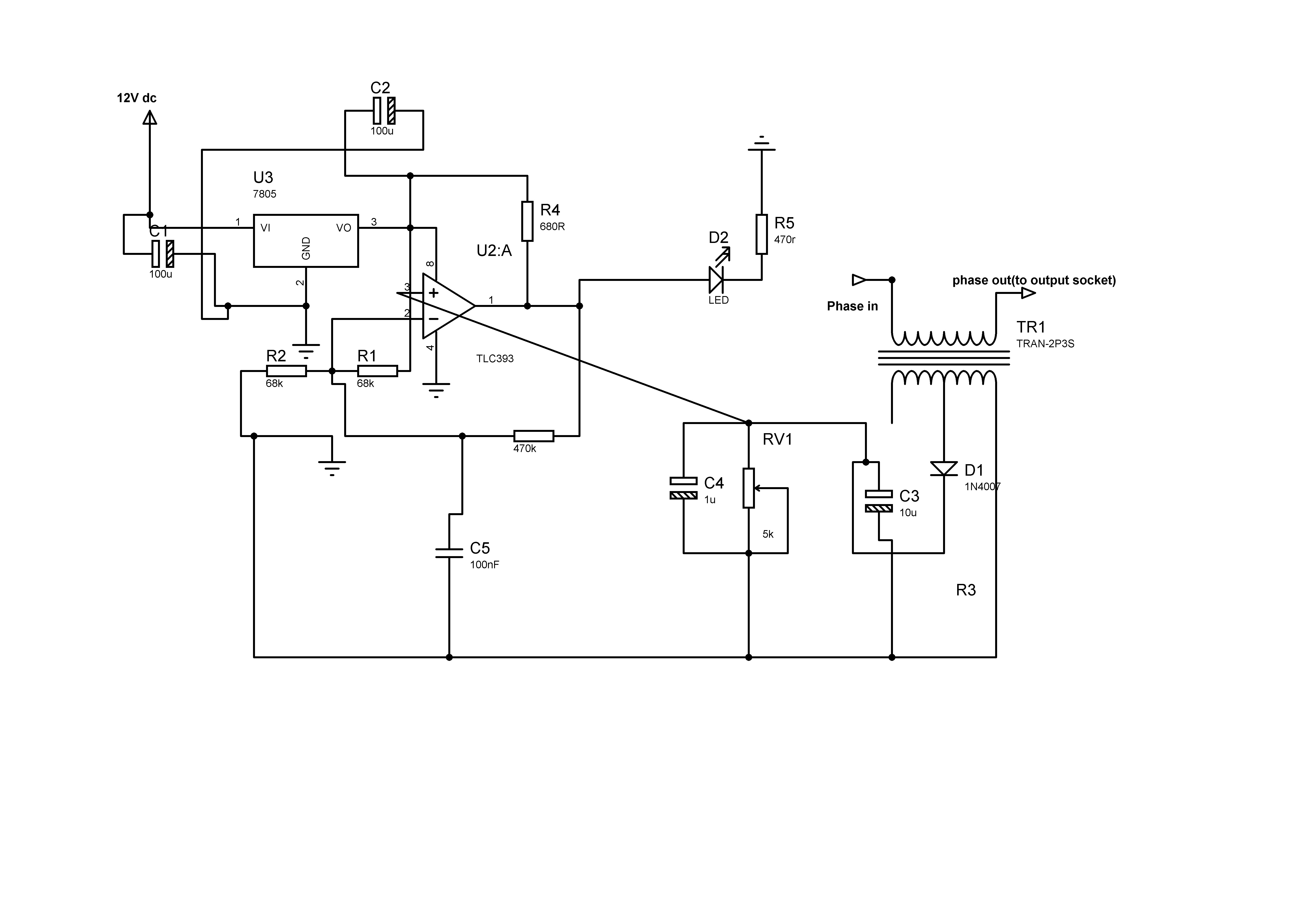
Ratio for CT(Current Transformer) depends upon,voltage.what's the ideal trans ratio of CT for stabilizers ?
voltage that we required on secondery side for operational amplifier(LM358,LM324 etc),or comparator.(393 and 339).
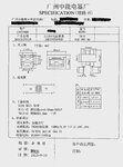
E And I type core used in C/T.For mid range and small voltage stablizers.
Babon size 1/4*1/4 inch(6.35mm*6.35mm) is suitable.
3 turns of swg,17 and 1000 turns of swg 40.
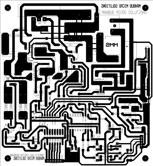
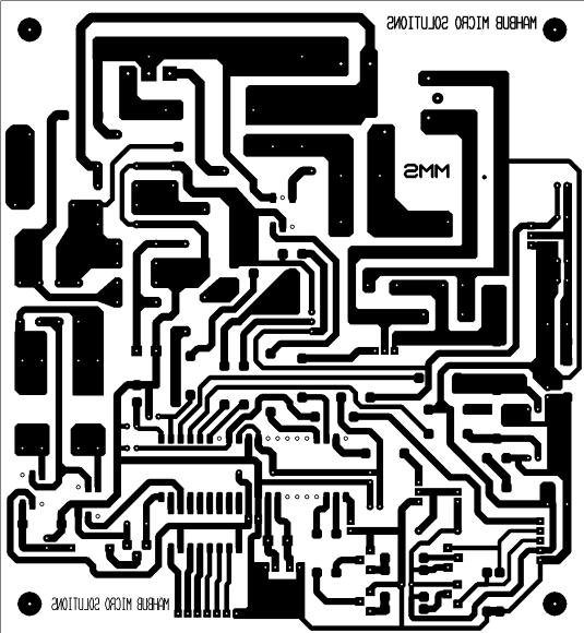
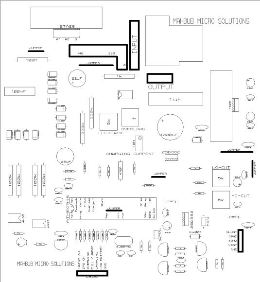
See attach files.