Continue to Site

Welcome to EDAboard.com

Welcome to our site! EDAboard.com is an international Electronics Discussion Forum focused on EDA software, circuits, schematics, books, theory, papers, asic, pld, 8051, DSP, Network, RF, Analog Design, PCB, Service Manuals... and a whole lot more! To participate you need to register. Registration is free. Click here to register now.

Queries on gm/id methodology

Status
Not open for further replies.
what exactly are u trying to achieve.....
@steadymind:please go through my last post in this link
https://www.edaboard.com/threads/201132/#post858084
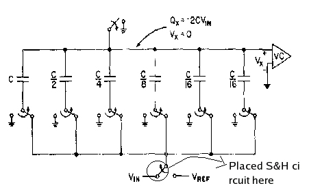
I've tried to simulate the following figure
74_1299132274.png

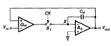
GBW of my OTA is 190MHz ,load capacitance is 500fF(Ch) and I don't how to find settling time of OTA,output satge is biased with 560uA and sampling error should be less than 18mV(resoultion of my ADC).What is the maximum sampling rate I can operate?
If I want to get a sampling rate of 250MHz then what do I need to do?
 

the settling time will the time taken to charge Cap (hold cap Ch) to the input value, the error ( sampled value - input value) can be between 18mV (resolution of ADC).

So 18mV is resolution of ADC.
allocate some percentage of this error to ur DAC (let say 50 %)
some percentage (25%) to sampling error in ur Ch. now this sampling error is made up of 2 main portions - DC gain error (ie 60 dB amplifer will have 1(max swing) /10^(60(gain)/20) ie <1m for 1V swing.) and settling error which is due to BW limitations.
now use these relations to adjust error so that u can meet ur specs.

GBW of OTA is 190MHz with 500fF load.. so Tgbw = 1/190MHz ~ 5nS
sampling time = half of 1/250MHz (assuming u have only half clock period for sampling) = 2nS = Ts
now allowing for some margin if ur OTA can sample ur input to Ch withing 1nS (0.5*Ts) with error less than (25% of 18mV -- as much as u allocate) then u are fine..

i hope this is clear ..

from my experience : in bootstrapped switch u have to look for sampling error to be constant irrespective of the input signal value... i never manged to achieve it dont know why
 
if ur OTA can sample ur input to Ch withing 1nS (0.5*Ts) with error less than (25% of 18mV -- as much as u allocate) then u are fine..
Thanks steady mind,I could get something from your explaination but not complete.Again my question is will an OTA with 190MHz GBW can sample signal in 1nS?? Sorry to ask same question again and again but I couldn't get clear picture !!

---------- Post added at 12:20 ---------- Previous post was at 11:25 ----------

@SteadyMind:I'm posting method I'm adapting,if there are any flaws please let me know.
I'm using charge redristribution architecture for DAC implemantation.During Sample mode Vin should be connected to DAC so I've inserted S&H in DAC as shown in figure
So during sample mode my sample and hold circuit should drive complete DAC capacitace(around 500fF).So if I use simple S&H circuit it can't able to drive that huge capacitance so need to insert some sort of analog buffer or a sample and hold circuit based on OPAMPS.
If you have understood my problem please give me a feasible solution.
 

OTA with 190MHz GBW has to respond as fast as your input signal within 1nS time frame, try simulating this.

as for ur architecture, my understanding is different i use the caps in the the DAC to be hold caps during the Vin sampling phase. I have a buffer (ota) which will be able to drive the caps in the dac to Vin with the sampling time within error limits .
 
OTA with 190MHz GBW has to respond as fast as your input signal within 1nS time frame, try simulating this.
I've simulated with input frequency of 2MHz output exactly follows input but for 200MHz signal output isn't near replica for input.What are the things that I need to do to improve its performance.

---------- Post added at 20:03 ---------- Previous post was at 19:54 ----------

i use the caps in the the DAC to be hold caps during the Vin sampling phase. I have a buffer (ota) which will be able to drive the caps in the dac to Vin with the sampling time within error limits .
Sorry!! I couldn't get the meaning of hold caps.If possible can you try to explain with timing diagram.
Thanks&Regards,
Ravinder.
 

definitely the gm/ID should be smaller than 1/VT. Transistor should be biased in the saturation region even in weak inversion. For weak inversion, make sure the vds larger than 4*UT. I guess you connected the transistor in the diode-connected way and drive it uing a current source, so, when reaching weak inversion, the transistor actually in linear region. Again, for weak inversion, make vds > 4*UT at least not Vds>Vgs-VT any more
 

I think u can use the caps in the DAC to be your hold caps and directly buffer(unity gain OTA) to drive the input voltage on these caps, i think this what u are also trying to do right ?
what are the specs for the ADC , input freq max , sampling freq, conversion time, number of bits.

for 200MHz input signal u need a bandwidth of atleast 200MHz, so increase ur OTA bw else roughly find out at what input freq ur output is different from input for 190MHz OTA. then u can scale ur OTA bw to match ur input sampling freq.
 

@SteadyMind:These are the specifications of ADC I'm targeting at :Maximum input frequency 500MHz and I wish to use two interleaved 6 bit ADCs(2 bits/step SAR) operating at 250MHz.I'm planning to allocate half of the conversion time of single ADC to sample&Hold and other half to DAC.

---------- Post added at 23:10 ---------- Previous post was at 23:03 ----------

for 200MHz input signal u need a bandwidth of atleast 200MHz, so increase ur OTA bw else roughly find out at what input freq ur output is different from input for 190MHz OTA. then u can scale ur OTA bw to match ur input sampling freq.
Yeah I've changed complete OTA,increased sizing of first stage so as to increase slew-rate but their sizing are coming to be very huge(80u).Now my OTA settling time is around 4ns(still doesn't reach my specs).output slew-rate isn't the same for both rising and falling(WHY??) and I do observe that there are overshoots when output it is going low and no overshoots when it is going high(??)

---------- Post added at 23:16 ---------- Previous post was at 23:10 ----------

directly buffer(unity gain OTA) to drive the input voltage on these caps
I think I need to detach buffer from DAC while it is sampling as the capacitors will be performing DAC operation(??)If this is true then how can I accomplish this task
 

schematic pic. if ur using 2 stage amp then output current mismatch b/w n and p will cause positive & neg. slew rate to be different....
overshoots normal as long as u have enough phase margin the overshoot will dampen out.
u just have to burn more current and have more bandwidth to meet ur specs.

---------- Post added at 19:53 ---------- Previous post was at 19:44 ----------

i dont understand ur architecture. as i see it there is a buffer that drives into 2 DAC capcaitor blocks in a time interleaved fashion. is that what are u using or something different
 

schematic pic. if ur using 2 stage amp then output current mismatch b/w n and p will cause positive & neg. slew rate to be different....
How can I make positive and negative slew-rates to be same(or how can match n and p)?
overshoots normal as long as u have enough phase margin the overshoot will dampen out.
Yeah we need to have enough phase margin,but why don't I get overshoots for rising output??
 

it will difficult to make the two slew rates to be equal but u can make them bigger than the minimum spec so that it meets it either way. u can get overshoot due to feed thru path of Cgd capacitance in the output device.
 
@SteadyMind:then I should get overshoots both for output rising(this I don't see) and output falling!!
 

true... can u post schematic or testbench , how are simulating slew rate, i perform open loop with negative i/p held at cm and then vary the positive i/p and check o/p.
 

I've shorted negative input of OTA with its output and applied a pulse signal at positive input of OTA!!
 

now it is exactly right bcoz now u have a feedback which will force negative input to go high as output rises due to positive input, what u want in slewing is to switch tail current thru one device of the input pair to the other, the feedback wont make this happen.
one reason why positive & negative slew are different is due to different paths the current takes.
 
i dont understand ur architecture. as i see it there is a buffer that drives into 2 DAC capcaitor blocks in a time interleaved fashion. is that what are u using or something different
Yeah you are right,I need to switch OTA output between two DACS.Can I use simple 2:1 mux for this switching as this needs to Carry around 1mA current
 
Last edited:

@SteadyMind:In the paper I've attached it is said that using reference buffers it is possible to achieve higher speeds than an OTA based switched capacitors.Is it true?And what are reference buffers,how are they used for switching??
 

Attachments

  • 2bits.pdf
    2 MB · Views: 63

Hi all,
I need formula to find the value of Shielded bottom plate capacitance(as shown in Figure) used to connect two DACs together.
 

Status
Not open for further replies.

Part and Inventory Search

Welcome to EDABoard.com

Sponsor

Back
Top