Continue to Site

Welcome to EDAboard.com

Welcome to our site! EDAboard.com is an international Electronics Discussion Forum focused on EDA software, circuits, schematics, books, theory, papers, asic, pld, 8051, DSP, Network, RF, Analog Design, PCB, Service Manuals... and a whole lot more! To participate you need to register. Registration is free. Click here to register now.

Why pad size smaller than hole size when in gerber file

Status
Not open for further replies.

amy87

Newbie level 5
Joined
Oct 29, 2010
Messages
10
Helped
3
Reputation
6
Reaction score
3
Trophy points
1,283
Activity points
1,354
Hi

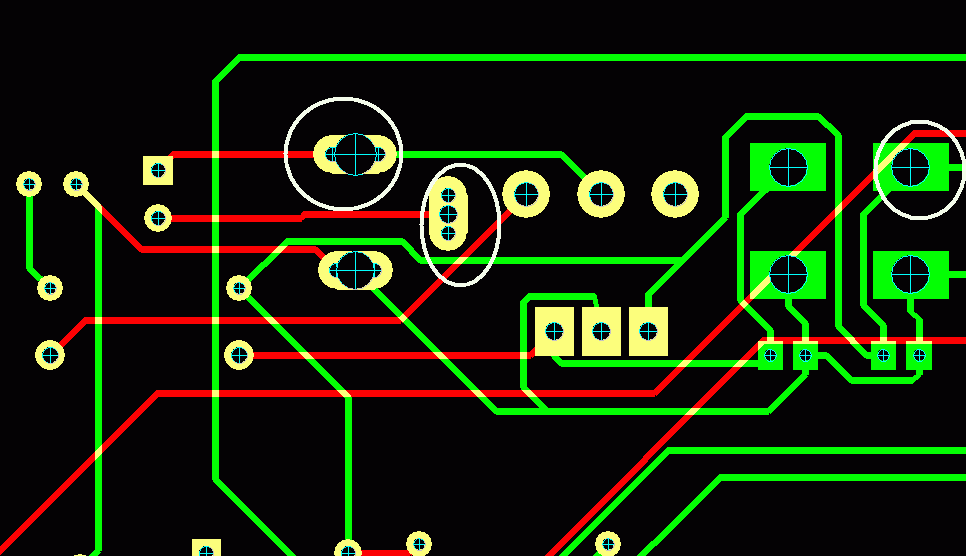
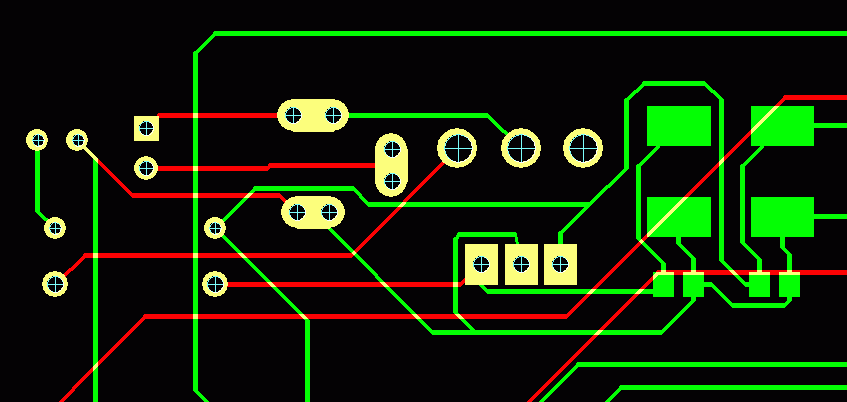
is anyone there know why the pad size become smaller than the hole size when in gerber file? I used dxp protel 2006 to design pcb. In layout, my pad size is bigger than the hole size, but when in gerber file, the opposite situation occurred. Is there anyone can help me solve this kind of problem?

Helpless
 

Which CAM tool you are using to view gerbers.
this might be because you ddont have set the NC drill table properly you have to set the drill sizes in CAM tool similar to that used in PCB.
 
Just to add something here, Amy has sent me the Gerber & drill files which I have loaded with GCprevue and the holes are definitely the wrong size (a fact confirmed by the PCB fabricator). Unfortunately it is not a simple matter on number of digits or units. I don't know Protel so have run out of ideas although we have tried several times to correct this. I am fairly sure it is too with how the drill files are created.

We need a Protel expert!

Keith
 
You should give some more information. Which file formats are you using for NC (provided, that the drill size is the problem, as Keith reported)? Does the file format include tool sizes with the drill data?

If I remember right, the default Protel/Altium workflow doesn't lead you to include the tool data during drill file generation. Because I'm only occasionally working with Altium, I simply added the sizes in a gerber tool, instead of further investigating the issue.
 
I used RS-274-X format. no, the tool sizes is separated from the drill data. but result still wrong. Is there have any setting during save the drill drawing. Coz yesterday Keith give me the manual for gerber file cretaed. But it din mention about the drill drawing. And is the setting for gerber file have something wrong. Please help me ..
 
is this issue available for all thru hole pads?? or to some particular pads??
for the first case we can suspect ncdrill generation methods or gcprevue.
if proble is occuring with some particular pads means some issue is there with your library/padstack.
Open the geber in GCprevue and check the property of copper pad in top layer,ensure it is same as the PCB data.
You can open the ncdrill file ( hole info) using a notepad and can ensure whether the data is correct.
If possible can you share the gerber files along with ncdrill data?
 
Hi, i still cannot install the GCprevue yet. So, still cannot check the drill file by myself. I can share the file, but the problem is i dono how to share it here?
Please Help me..
 
Hi, i still cannot install the GCprevue yet. So, still cannot check the drill file by myself. I can share the file, but the problem is i dono how to share it here?
Please Help me..
you can use any gerber viewer to check the gerber. GCprevue is a free ware.
gcprevue down load link: **broken link removed**

to share the files you first zip all gerber files ( top,bot,silk,...) using winzip or win rar . then click on the Go advanced button . there you will get options to upload files.
 
Ok, i post the drill file and gerber file here. Hope can help me ...
 

Attachments

  • NEW.zip
    128.7 KB · Views: 137
hi Amy,

issue is with your CAD data itself.
check the file "C:\Users\Amy\Documents\NEW\cam1.rpt" or 'cam1.drl' . it says you have 28 different types of drills I think some mistake is there in your ncdrill generation (.drl file) procedure.
as per this data the smallest drill size in your design is 0.050"(1.27 mm) and it is for vias!!!
Please check the .drl generation procedure again..
 

Yes, I double checked the drill files to make sure GCprevue was showing me the correct values (it sometimes lies) and found the same thing. Unfortunately I don't know Protel so cannot talk Amy through fixing it.

Keith
 

I agree, that the fault is apparently already present in the Protel design. I scaled cam1.drl to 50% and got partly reasonable drill sizes. There are however several details that aren't manufacturable as is, e.g. multiple drills in a pad. I also don't understand, why there are 14 different drill files have been produced, most of them empty. The four containing data are almost identical, except for an obviously erratic drill in a SMD pad.

The PCB outline is apparently missing from the gerber plots, it would be expected in *.gm15 according to Protel/Altium standard.

I must add, that I'm no used to operating Protel with imperial (inch) units, the drill size confusion may be related to it.

To make us understand the nature of the problem, you should possible show a screenshot of the layout, or post 68_design.pcbdoc.


P.S.: To add a more general comment: I seriously doubt, if the design will work reliably with the present supply and ground wiring and effectively no bypass caps near to most logic and memory ICs. It's also strongly recommended to use wider traces for power supply. When making logic circuits on a two-layer PCB, I would always try to wire a least ground and possibly vcc in a grid topology.
 
Last edited:

Act I dono where can change dy. There are not many step need to do in order to create the gerber file. But about the drill file, i din set any thing because dono where can do setting. Can tell me where can do the setting?
 

check the link
https://www.edaboard.com/threads/12042/
hope this will work for you.

If everything fails means simply edit the values in cam1.drl using a text editor and save it (eg:T28C0.0500 means Tcode 28 with 0.050" drill dia edit it to T28C0.0100 ie Tcode 28 with 0.010" drill dia)
 

Have you done a drill drawing to let the manufacturer know what size holes on what pads you want?

Edit: Why so many drill files?

Surely you only need 2, 1 for plated and one for non plated.
 
Last edited:

View attachment pcb file.zipThanks for help. I post the pcb file here... Hope can find the actual problem through it. Cause act the setting followed the instruction dy. The problem still occurred at all.
 

Unfortunately, I don't have the said Protel version. With recent Altium versions, the drill tools are apparently assigned correctly. So I wonder, if it's a problem of a specific Protel version.


There seems to be a change in the processing of the milled J1 slots, Altium sees only two drills at the slot ends. The three drills for each pad in your drill file version cause possibly problems in PCB manufacturing, as already mentioned. Personally, I prefer larger round pads for those DC connectors, because they can be produced by any manufacturer without problems.
 

Attachments

  • 68K_design.TXT
    8.9 KB · Views: 63
Last edited:

Hi,

I think before this i misunderstand already. I direct save the drill file from gerber file (camtastic) there, so the size of drill act is the total size for hole and pad. Now, i save the drill file from NC drill file there, the size is correct. So, izzit means that wehave one drill file only?
 

As far as I see, you don't have unplated holes in your design, so one NC drill file is correct.

But you should define a board outline in your Protel design, and check, if the PCB manufacturer
can make milled throughplated slots for connector J1 from your present drill data.
 

Status
Not open for further replies.

Part and Inventory Search

Welcome to EDABoard.com

Sponsor

Back
Top