Continue to Site

Welcome to EDAboard.com

Welcome to our site! EDAboard.com is an international Electronics Discussion Forum focused on EDA software, circuits, schematics, books, theory, papers, asic, pld, 8051, DSP, Network, RF, Analog Design, PCB, Service Manuals... and a whole lot more! To participate you need to register. Registration is free. Click here to register now.

Where and how the NF and Gain circle move if the source degen inductor changes?

Status
Not open for further replies.

cmosbjt

Full Member level 5
Joined
Apr 25, 2004
Messages
250
Helped
10
Reputation
20
Reaction score
2
Trophy points
1,298
Location
USA
Activity points
2,293
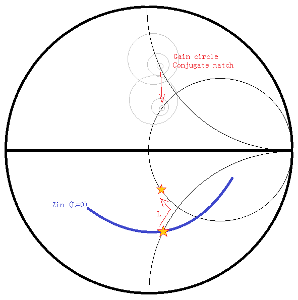
Interview: Where and how the NF and Gain circle move if the source degen L changes?

For a simple inductive source/emitter degeneration single ended LNA configuration. Where is the NF and Gain circle located and how do they move when the source/emitter inductor changes it value, and why?
 
Last edited:

Does anyone know the answer?

During the interview, I drew the Gain and NF circles based on my experience of several LNA designs. But the guy kept asking why they are located there and why they move like that.

I am not sure if that guy knows the CORRECT answer, but if he does then there must be a "common sense" answer that an RF/MW IC design engineer is supposed to know.

Can anyone help?

---------- Post added at 18:30 ---------- Previous post was at 16:32 ----------

I just figured out the Gain circle location and movement:

Zin≈(gm/Cgs)*L + s*L + 1/(s*Cgs)

when L increase, the real and imaginary part of Zin increase, then the gain circle will move as shown in this picture. Not sure if this is the correct answer. But I still can't figure out the noise circle (or NFmin) movement. I think the NF data is more empirical.

76_1289150782.png
 

NFmin is related to Zin.. ( or Yin)
I don't remember the equation that relates NFmin to Yin by heart.
For more information, look at "Radio Frequency Integrated Circuit Design, John Rogers, Calvin Plett , Artech house"..
 

Can't find any related info in that book. I mean, come on, this is an interview question, is it supposed to have a well known answer?
 

Here is what I find in this book. Very complicated equations for the NFmin of a common emitter bipolar amplifier. It is hard to tell where the noise figure circles are and let alone it is not even an inductive source degen configuration.

67_1289358420.png
 

Here is what I find in this book. Very complicated equations for the NFmin of a common emitter bipolar amplifier. It is hard to tell where the noise figure circles are and let alone it is not even an inductive source degen configuration.

67_1289358420.png

But it tells you-approximately- why NFmin is related to input impedance parameter or in otherwords why NFmin is changed with intrinsic input parameters of a transistor.You can extract an answer from this equation for your case.
I suggest you follow the same methodolgy to extract an equation for emiter/source coil regenerated amplifiers.Because when you connect a coil at emitter, input impedance will consist of intrinsic transistor parameters(Cpi and rb ) and coil reactance that's why NFmin will be changed with these two input impedance parameters.
 

Status
Not open for further replies.

Part and Inventory Search

Welcome to EDABoard.com

Sponsor

Back
Top