Continue to Site

Welcome to EDAboard.com

Welcome to our site! EDAboard.com is an international Electronics Discussion Forum focused on EDA software, circuits, schematics, books, theory, papers, asic, pld, 8051, DSP, Network, RF, Analog Design, PCB, Service Manuals... and a whole lot more! To participate you need to register. Registration is free. Click here to register now.

why do we need pad rings?

Status
Not open for further replies.

mona123

Member level 5
Joined
Jun 10, 2010
Messages
87
Helped
3
Reputation
6
Reaction score
3
Trophy points
1,288
Activity points
1,898
why do we need pad rings for gnd and vcc? thanks.
 

could you show me what does pad rings look like with a picture?
i even never heard about pad ring before, a ring surrounding the pad?
 
mona123 said:
why do we need pad rings for gnd and vcc? thanks.
"Pad ring" or "pad frame" usually is understood as the periphery (or circumference) of a chip which contains all the bond pads. It also includes several wide tracks for global power supply nodes as, e.g., gnd! , vdd! , possibly separate ones for analog and digital pwr supplies and/or dedicated ESD nodes. In most cases these wide parallel tracks are designed as rings within the pad ring in order to facilitate short access lengths to these global low-resistive nodes.
See here an example for a pad ring, where the wide ring tracks for GND and VDD are visible (from
 
i see, pad ring is the wide power supply and ground bus :)
 
prcken said:
i see, pad ring is the wide power supply and ground bus :)
Right. Additionally it includes the I/O drivers, ESD structures, and the bond pads.
 
  • Like
Reactions: diaz080

    mona123

    Points: 2
    Helpful Answer Positive Rating

    diaz080

    Points: 2
    Helpful Answer Positive Rating
Thanks erik for the answer but my question was why do we need a ring to connect all pads? is to keep the ground of different parts of the ckts at same potential or something?
 

mona123 said:
Thanks erik for the answer but my question was why do we need a ring to connect all pads? is to keep the ground of different parts of the ckts at same potential or something?

as erik mentioned “In most cases these wide parallel tracks are designed as rings within the pad ring in order to facilitate short access lengths to these global low-resistive nodes.”


when you do floorplan for a chip, you should consider the positions of each block (including the digital block), IO pins and especially power pins and ground pins. you are not allowed to put power and ground pins whereever you like to due to limited package pins and costs. so usually you place several power pads or ground pads at one or two places for certain blocks in the chip, and with wide metal (usually ≥ 20µm for one metal layer with several metal layers, i call it power bus and ground bus) running around the chip to each block connected. the current flowing in power bus and ground bus is large so that wide metal is needed to reduce IR drop, and it's essential for ESD consideration. sometimes, we also add a dedicated ESD bus for large scale chips in oder to provide an additional ESD path.
 

thanks prcken. can u tell me how do these buses help for esd?
 

ESD bus connects different power buses or ground buses via dual diodes, due to increased die
size and package pins, full chip ESD protection may become a problem, ESD bus is a good method to enhance full chip ESD protection performance, ESD bus is a bridge when ESD zapping is happened between different power domains.

i have attached a picture below for your understanding.
10_1279366213.jpg

this is taken from a reference:
Ming-Dou, K., C. Hun-Hsien, and C. Tung-Yang. ESD buses for whole-chip ESD protection. Proceedings of the 1999 IEEE International Symposium.

and there are some other literatures also talked about this.
 

    mona123

    Points: 2
    Helpful Answer Positive Rating
Thanks prcken and erik your answer helped me understand why you may need bus all around the chip. I have clicked helped me for both of you.

prceken, I have couple of questions though. I am gonna get the paper you mentioned somehow and read it.

1) why do you need separate esd buses. They all must be connected to ground for the discharge, isn't it?

2) What for are these esd clamps between esd buses? what kind of circuit is there for esd clamps?

3) I see CMOS inverters at the pads. How do they help in esd?

Thanks. will aprreciate your answer.
 

1) why do you need separate esd buses. They all must be connected to ground for the discharge, isn't it?
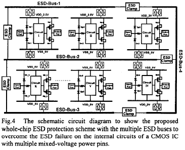
actually that depends, the author used separate ESD buses for better isolation between each blocks at normal working conditions. it need at least two the so called ESD clamps from one block to aonther block. All the ESD buses are floating, they are intended to provide a ESD path for ESD stresses happened between two separate power domains, for example ESD test zapping combination is from VDD1 to VDD2, there are at least two main ESD paths to discharge the large ESD current, i.e VDD1->ESD bus->VDD2 and VDD1->GND1->ESD bus->GND2->VDD2
2) What for are these esd clamps between esd buses? what kind of circuit is there for esd clamps?
as aforementioned add ESD clamps for better isolation at normal working operation.
this ESD clamps should be bi-directional, usually dual diodes are used, and other area efficient and robust ESD devices like dual directional SCR is also reported.
3) I see CMOS inverters at the pads. How do they help in esd?
the inverters are output buffers, dont necessarily be an inverter there, maybe a source follower, maybe an open drain output, the author just took the inverter for illustration, they are to be protected and can be self-protected, usually the sizes of the inverters are large and layed-out according to ESD rule
 

you mentioned ~20um as bus width, is there any rule of thumb for spacing between the rings?
 

oermens said:
you mentioned ~20um as bus width, is there any rule of thumb for spacing between the rings?
no, just make sure not to violate DRC
 

Tha nks. Can you please explain your statement "there are at least two main ESD paths to discharge the large ESD current, i.e VDD1->ESD bus->VDD2 and VDD1->GND1->ESD bus->GND2->VDD2".

How VDD to VDD is discharge path? I am used to thinking that you can only discharge through ground. Also where is GND here ( or may be the picture is small so I can't see?).
 

Can you please explain your statement "there are at least two main ESD paths to discharge the large ESD current, i.e VDD1->ESD bus->VDD2 and VDD1->GND1->ESD bus->GND2->VDD2".
there are several ESD paths for ESD current flowing from one pin (VDD1) in respect to another pin(VDD2), at this time ground pin is floating, ESD current is passing through GND bus from one terminal to another.

How VDD to VDD is discharge path? I am used to thinking that you can only discharge through ground. Also where is GND here ( or may be the picture is small so I can't see?).
when you do ESD Zapmaster testing, you have to define zapping combinations, All pins to GND is just one set of test combinations. All pins to VDD1 is another set of combination, VDD2 to VDD1 zapping is included in this set.
 

Status
Not open for further replies.

Part and Inventory Search

Welcome to EDABoard.com

Sponsor

Back
Top